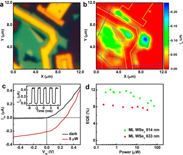
Figure 4.
Photoresponse of the WSe2/MoS2 heterojunction p–n diode. (a) Optical microscpope image of the WSe2/MoS2 heterojunction. (b) False color scanning photocurrent micrograph of the WSe2/MoS2 heterojunction device acquired at Vds = 0 V and VBG = 0 V under irradiation 514 nm laser (5 μW). The purple square dotted line outlines the ML-WSe2 and the dark purple square dotted line outlines the BL-WSe2. The blue circle dotted line outlines the MoS2 and the golden solid line outlines the gold electrodes. Photocurrent were observed in the entire overlapping junction area. (c) Experimental output (Ids–Vds) characteristic of the vertical heterojunction device in the dark (black) and under illumination (wavelength: 514 nm; power, 5 μW). Inset, temporal response of the photocurrent generation under 514 nm illumination (10 μW). (d) Power-dependent EQE of the heterojunction device under 514 and 633 nm laser excitation wavelengths at Vds = 0 V and VBG = 0 V. A maximum EQE of 12% was observed.

