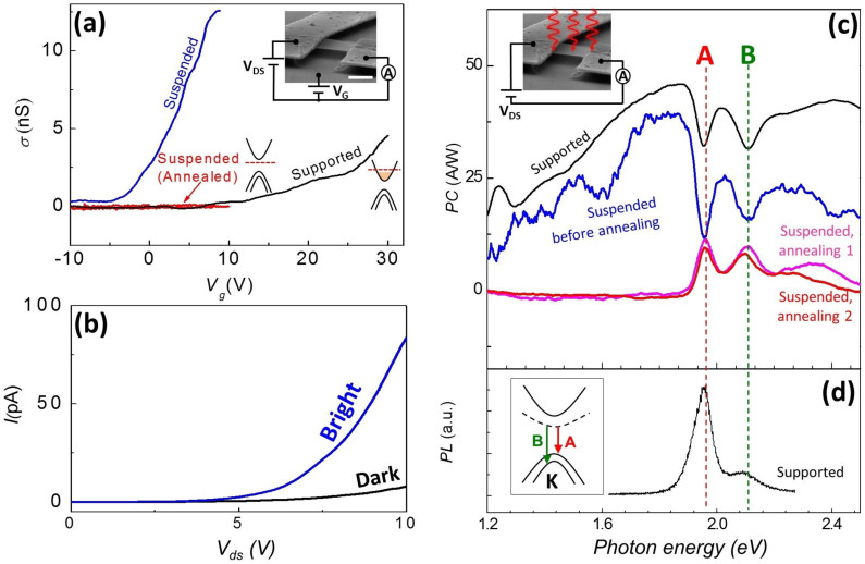
Figure 1. Effects of substrate and thermal annealing on conductance and photocurrent of suspended MoS2.
(a) Gate-dependent conductance of supported, suspended, and suspended annealed 1L-MoS2 device #1 at T = 300 K. Inset: Image of the device. The scale bar is 1 μm. Schematically drawn band diagrams show the position of the Fermi level (red dashed line). (b) Dark and bright electrical response of an annealed suspended device #2 at T = 77 K. Illumination intensity is ~3 pW/μm2 and wavelength is λ = 430 nm. (c) Photocurrent (PC) spectrum of a supported and suspended MoS2 device #1 at different stages of thermal annealing at T = 77 K. (d) Photoluminescence spectra for a supported MoS2 device #1 at T = 300 K. Since PL spectra were recorded at room temperature, we manually blue-shift them by 150 meV to allow comparison with PC spectra obtained at T = 77 K (see Supplementary Information, S5 for details). Inset: Bandstructure schematics of MoS2 near K-point illustrating the origin of band-edge excitons. The dashed line represents excitonic states.

