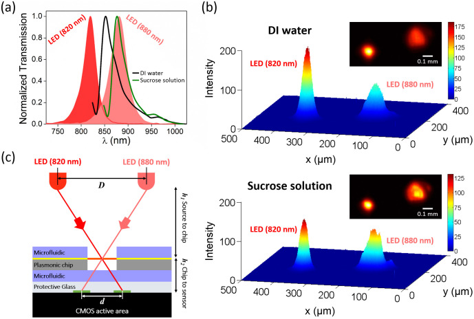
Figure 2. Operation principles of dual-wavelength plasmonic detection platform.
(a) Solid curves: Spectral variation in the plasmonic mode supported by the nanohole arrays under DI-water and sucrose solution 1.1 M. Filled curves: The spectral responses of the two LEDs employed by the lensfree on-chip imaging platform with peak wavelengths of 820 nm and 880 nm. (b) 3D visualization of the intensity of the dual diffraction pattern of the nanohole arrays formed by LED illuminations at 820 nm and 880 nm under DI-water and sucrose solution, respectively. Figure inset: Raw lensfree dual diffraction image for a single plasmonic pixel. (c) Schematic illustration of the generation of dual-diffraction patterns at the detector plane of the lensfree platform. LED separation distance: D, dual diffraction pattern separation distance: d, LED to plasmonic chip: h1, and plasmonic chip to on-chip imager active area: h2.

