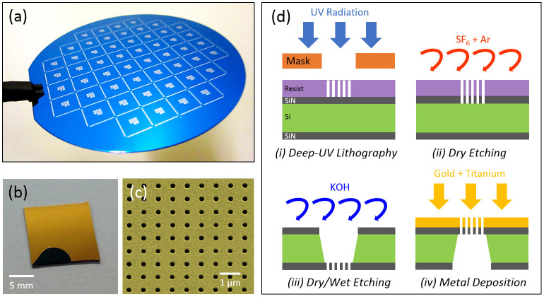
Figure 3. Deep-UV Lithography based high-throughput fabrication of plasmonic nanohole arrays.
(a) Photography of the wafer after deep-UV and dry etching steps. (b) Single plasmonic chip containing eight plasmonic pixels. (c) SEM image of the nanohole array with a hole diameter of 200 nm and an array period of 600 nm. (d) Fabrication steps of the nanohole arrays on free-standing silicon nitride membrane.

