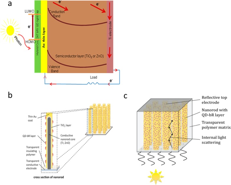
Figure 1.
(a) Planar structure of the solid-state photovoltaic device. (b) Illustration of a nanowire array showing the conductive core, covered, respectively, by TiO2 (or ZnO) semiconductor metal oxides, Au, and QD-bR dye layers. Panel c illustrates how the nanowire array can be packaged to include a lower transparent electrode, a transparent polymer matrix to provide mechanical stability and flexibility, and a top reflective electrode. The polymer matrix can include particles with index of refraction differing from the matrix to further enhance internal reflections.

