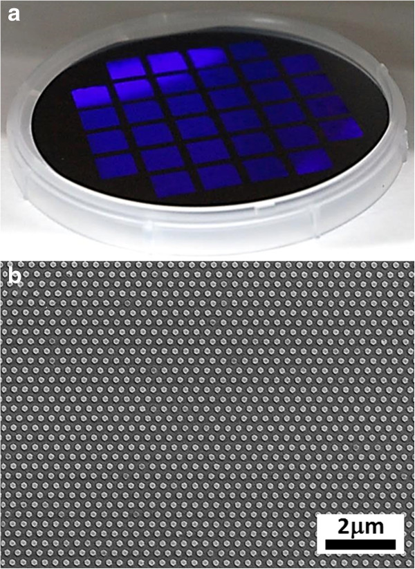
Figure 3.

Photograph of nanoimprinted 4″ Si wafer (a) and SEM image showing long-range order of corresponding nanostructures (b). The wafer in (a), produced by SRNIL, was deliberately tilted at an angle to bring out the violet-blue tinge arising from the optical diffraction caused by the highly ordered nanoimprinted hexagonal studs of 300-nm periodicity.
