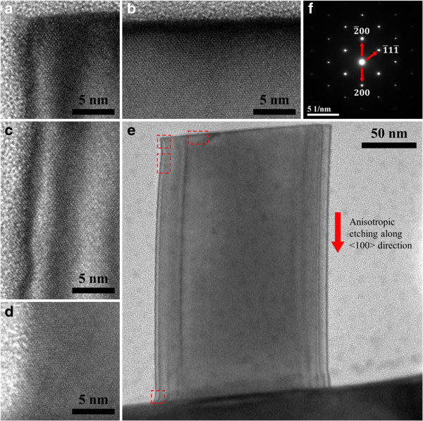
Figure 7.

HR-TEM images of metal-catalyzed electrolessly etched Si nanostructure (after a 60-s etch and removal of NIL mask). (a) Top left corner. (b) Top surface. The well-defined and flat top interface is a consequence of the resistance of the NIL mask against chemical attack. (c) Left sidewall near the top surface. The etched sidewall shows a higher extent of surface roughness of about 3 nm due to attack by the HF/H2O solution. (d) Left sidewall towards base of nanostructure. Surface roughness is smaller due to shorter exposure to etching solution. (e) TEM image of the entire MCEE Si nanostructure. Red-outlined boxes show the locations of where the magnified HR-TEM images were taken. The etching proceeds preferentially along the <100 > direction. (f) The single crystal quality of the Si is evident from the SAED pattern.
