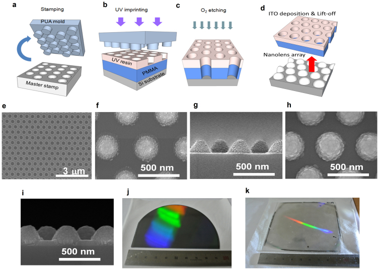
Figure 1. Formation of nanolens-arrays.
(a–d), Schematics of nanoimprint method. (e), A scanning electron microscopy (SEM) image of PMMA hole-arrayed patterns. SEM images of ITO-nanolens-arrays (f, g), and ITO-nanolens-arrays with an additional 80 nm-thick ITO film (h, i). Photos of ITO-nanolens-arrays on Si wafer (j) and on glass (k). For the Si wafer, the n-p junction was previously formed using a doping process (See Methods).

