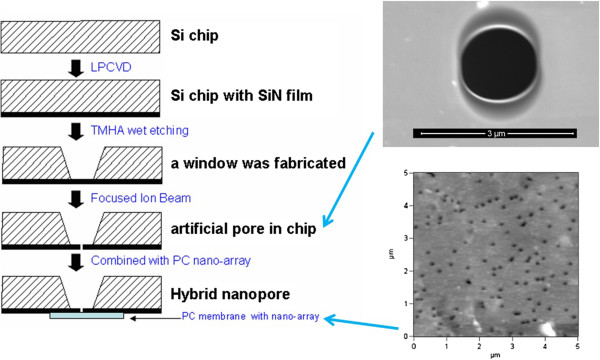
Figure 2.

Illustration of the integration process of micropore. (1) Si3N4film on one side of the Si chip was obtained by LPCVD method. (2) A window on the top of chip at Si side was fabricated by wet etching. (3) Artificial micropores on the Si3N4film were fabricated by FIB. (4) PC membrane was covered on the Si3N4pore and sealed using PDMS. The inset in the top right corner is the SEM image of Si3N4 micropore; the inset in the lower right corner is an AFM image of the PC nanopore arrays.
