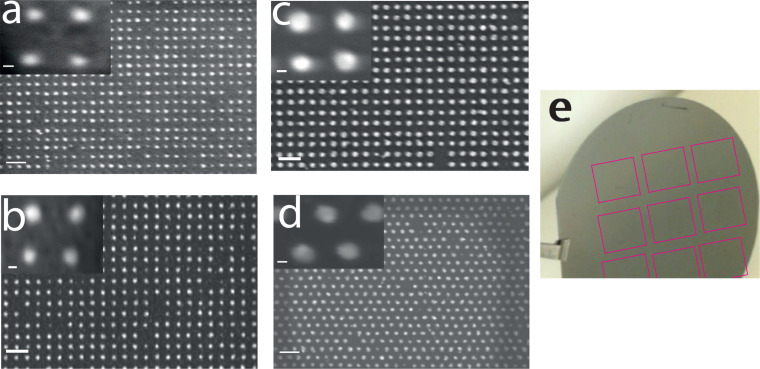
Figure 2.
Scanning electron microscope (SEM) images of the gold nanodot arrays fabricated by (a) the “conventional” method with an exposure dose of 16000 µC/cm2 (4 fC/dot), (b) the “advanced conventional” method with an exposure dose of 16000 µC/cm2 (4 fC/dot) (c) the DOTF method with an exposure dose of 160 µC/cm2 (4 fC/dot) (d) the “sequence” method with an exposure dose of 12000 µC/cm2 (3.5 fC/dot). The beam current is set to 10 nA for the three techniques. The scale bar is 100 nm for the 4 SEM images and 10 nm for zoomed SEM images shown in inset. (e) Picture of a 3 inch wafer where 9 sequences of 1 cm2 have been written using DOTF and “sequence” methods. Given the small contrast provided by the 8 nm thick gold nanoparticles, these arrays are indicated by pink squares.

