Abstract
Power transfer efficiency (PTE) and power delivered to the load (PDL) are two key inductive link design parameters that relate to the power source and driver specs, power loss, transmission range, robustness against misalignment, variations in loading, and interference with other devices. Designers need to strike a delicate balance between these two because designing the link to achieve high PTE will degrade the PDL and vice versa. We are proposing a new figure-of-merit (FoM), which can help designers to find out whether a two-, three-, or four-coil link is appropriate for their particular application and guide them through an iterative design procedure to reach optimal coil geometries based on how they weigh the PTE versus PDL for that application. Three design examples at three different power levels have been presented based on the proposed FoM for implantable microelectronic devices, handheld mobile devices, and electric vehicles. The new FoM suggests that the two-coil links are suitable when the coils are strongly coupled, and a large PDL is needed. Three-coil links are the best when the coils are loosely coupled, the coupling distance varies considerably, and large PDL is necessary. Finally, four-coil links are optimal when the PTE is paramount, the coils are loosely coupled, and their relative distance and alignment are stable. Measurement results support the accuracy of the theoretical design procedure and conclusions.
Index Terms: Charging electric vehicles, implantable microelectronic devices, inductive, mobile devices, power transfer efficiency (PTE), wireless power transmission
I. Introduction
Inductive power transmission has received considerable attention in recent years for use in a wide variety of applications that require contactless energy transfer over short distances. Depending on the application, the power level varies from microwatts in radio frequency identification tags [1], [2], to milliwatts in implantable microelectronic devices (IMDs), such as cochlear implants [3]–[5], watts in handheld mobile devices (HMDs) [6]–[10], and kilowatts in charging electric vehicles (EVs) [11], [12].
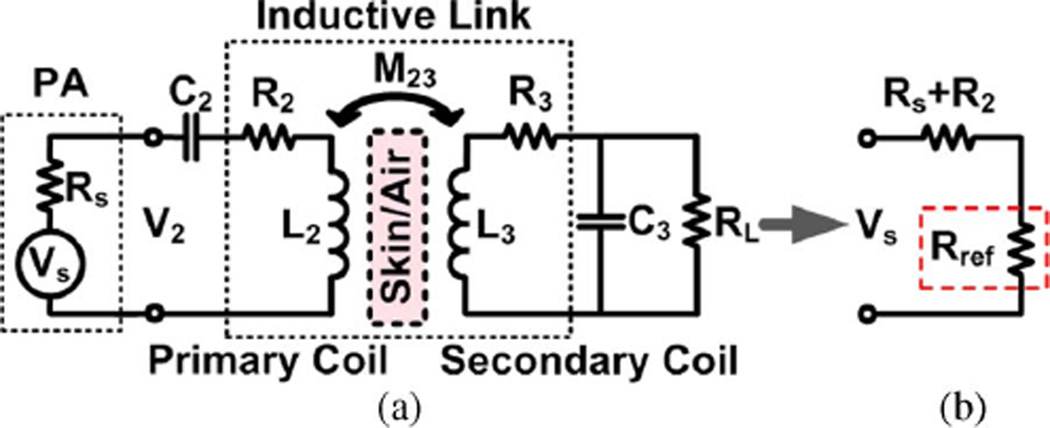
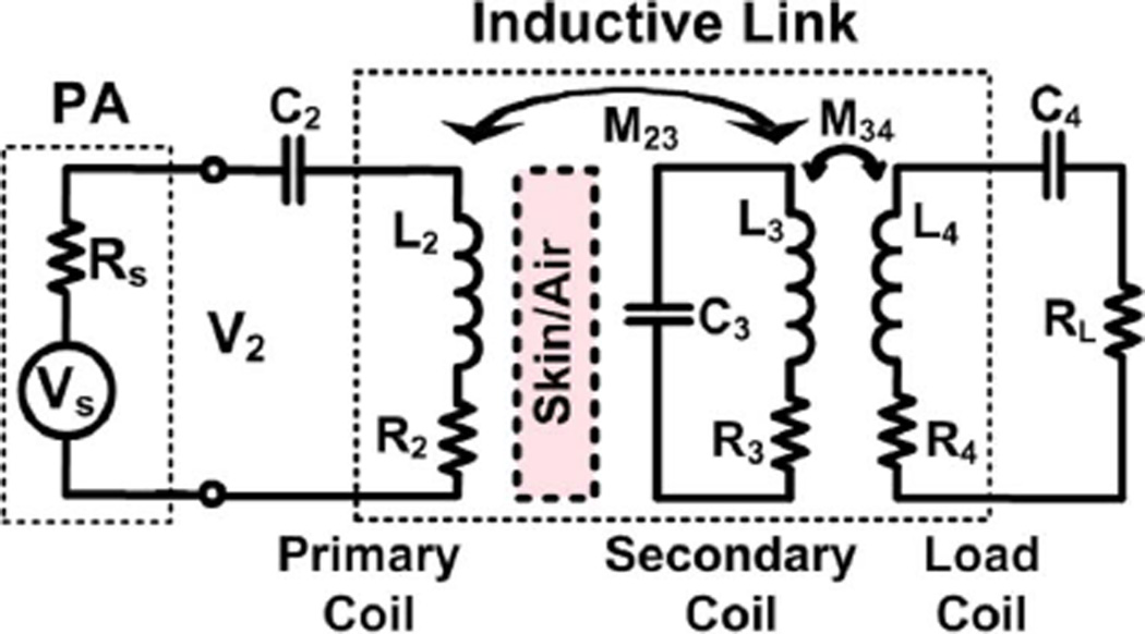
In a generic power transmission link, shown in Fig. 1(a), a highly efficient power amplifier (PA) on the transmitter side (Tx) drives the primary coil, which is mutually coupled to a secondary coil on the receiver side (Rx) to power up the load (RL). In the rest of this paper, RL represents the ac equivalent of the power conversion circuitry and the dc load.
Fig. 1.
(a) Lumped circuit model for a generic two-coil inductive power transmission link with the PA loss modeled as Rs. (b) Equivalent circuit at resonance showing the reflected load from the secondary loop onto the primary loop.
A key design requirement in all the above applications is to provide sufficient power delivered to the load (PDL) while maintaining high power transfer efficiency (PTE). High PTE is required to reduce 1) heat dissipation within the coils, 2) exposure to electromagnetic field, which can cause additional heat dissipation in the power transmission medium, 3) size of the main energy source (e.g., battery), and 4) interference with nearby electronics that is necessary to satisfy regulatory requirements [13]–[15]. At the same time, the link should deliver sufficient power to the load while considering practical limitations of the energy source and the PA. When RL is constant, the PDL would be equivalent to the inductive link voltage gain all the way from the source to the load. Increasing the source voltage, Vs in Fig. 1(a), to increase the PDL can reduce the driver efficiency, require larger transistors in the PA, and make it more difficult and costly to meet the safety requirements [16].
Several methods have been proposed for designing wireless power transmission links. In [2], [17], and [18], geometries of the primary and secondary coils, L2 and L3 in Fig. 1(a), have been optimized to achieve the maximum voltage on the load, and consequently a high PDL. PDL is a key design merit when the space is limited and coils need to be miniaturized, such as in the IMD applications. Similarly, design and geometrical optimization of the two-coil inductive links based on the PTE have been widely studied [19]–[24]. The approach proposed in [25] is somewhat different by first designing L3 to maximize the PTE for a given RL, and then optimizing L2 to achieve the desired voltage gain from source to the load, and consequently improve the PDL. However, the literature still lacks a clear figure-of-merit (FoM) that can incorporate both the PTE and the PDL, and guide designers to give proper weight to each of these important but contrasting parameters. A well-defined FoM can provide designers with much needed insight on how to optimize their inductive power transmission links based on the application requirements.
Recently, multi-coil power transmission links have been proposed and studied to further increase the PTE, particularly at large coupling distances, d23 [26]–[30].We have also presented the analysis, design, and optimization of the two-, three-, and four-coil inductive links based on the PTE and analyzed the PDL of these links [16].We have shown that there is a compromise in the four-coil links between simultaneously achieving high PTE and PDL at small and large distances, respectively. This can also be seen in [29] where the PTE has been purposely reduced at smaller d23 from 70% to 10% to achieve a high PDL at large d23. However, our proposed three-coil link has achieved both high PTE and PDL [16].
In this paper, we propose a new FoM, which serves two purposes. First, it guides designers toward inductive power transmission links with the highest possible PTE and PDL. Second, it helps the designer to choose between the two-, three-, and four-coil link options for a given application. In the following section, we have introduced the new FoM and the tradeoffs between achieving high PTE and PDL, simultaneously, in a two-coil inductive link. Section III presents the two-coil inductive link performance comparison when designed based on PTE, PDL, and FoM for different source and load scenarios. Section IV describes the design and optimization procedure for the three- and four-coil inductive links based on the FoM. Calculation and measurement results for the HMD charging and theoretical calculation for EV applications are included in Section V, followed by the discussion and concluding remarks in Sections VI and VII, respectively.
II. New Fom for Inductive Power Transmission
In Fig. 1(a), key parameters that affect the design of this link from the energy source to the load, aside from the coils are: Vs, power required by the load (PL), PA supply voltage (VDD), Rs (representing the PA loss), PA transistor breakdown voltage, and safety limits for the application [21]. In a class-E PA, zero-voltage-switching allows for high power efficiency with peak voltages across the primary coil and the PA transistor that are 1.07 and 3.56 times VDD, respectively [31]. Therefore, when the application requires a large PL, Rs should be reduced to make sufficient power available from the source, , at a reasonable Vs and VDD [21], [29]. Unfortunately, to achieve a high PTE, the delivered power to L2 would be much smaller than Paυ because the impedance matching on the Tx side reduces the PA efficiency to 50%. Utilizing large transistors to reduce Rs results in increased dynamic switching losses in the PA [25]. Therefore, the power transmission link should be designed in a way that it achieves high PTE and also provides sufficient PDL, while considering practical limitations of the PA circuit design.
It can be shown that the highest PTE and PDL for the inductive link, shown in Fig. 1(a), can be achieved when both LC tanks are tuned at the same resonance frequency, [25]. At resonance, the effect of the Rx on the Txcan be modeled by the reflected impedance
| (1) |
where , M23 is the mutual inductance between L2 and L3, and Q3L = Q3QL/(Q3 + QL), Q3 = ω0L3/R3, and QL = RL/ω0L3 for parallel load connection, which is often referred to as the load quality factor [1]. At resonance, the primary loop can be simplified to the circuit shown in Fig. 1(b).
To calculate the PTE at resonance, we should consider that the power provided by the PA (Vs) divides between Rs + R2 and Rref, and that portion of the power delivered to Rref, i.e., the power that is received by the secondary loop, divides between R3 and RL, which are the only power-consuming components. These assumptions lead to
| (2) |
where Q2 = ω0L2/(Rs + R2) [25]. The first and second terms in (2) correspond to the power division between Rs + R2 and Rref, and R3 and RL, respectively. Therefore, according to (2), in order to achieve the highest PTE, Rref should be maximized.
PDL can be calculated by multiplying the power provided by Vs, i.e., , with the PTE from (2)
| (3) |
It can be seen in (3) that PDL does not necessarily increase by maximizing Rref. Taking the derivative of (3) with respect to Rref indicates that the maximum PDL at a certain coupling distance, d23, is achieved when Rref = Rs + R2. Under this impedance-matched condition, PTE ≤ 50%, because at least half of the power is dissipated in Rs + R2.
To better understand and manage the necessary compromise between the PTE and PDL when designing an inductive power transfer link, we propose a new FoM
| (4) |
where n depends on the importance of the PTE versus PDL in a particular application. Interestingly, the FoM unit is in Siemens, which implies how conductive the wireless link is to electric power transfer. The FoM for a two-coil link can be derived from other circuit parameters in Fig. 1 by substituting (2) and (3) in (4)
| (5) |
According to (2), the PTE profile of a two-coil link is a monotonically decreasing function of the coils’ coupling distance, d23 [16]. The PDL and FoM profiles, on the other hand, can be maximized at a particular d23 by calculating the derivatives of (3) and (5) with respect to k23, respectively,
| (6) |
By substituting k23,FoM in (2) and (3), one can find the PTE and PDL of the two-coil link when the FoM is maximized at a particular d23
| (7) |
These equations do not consider any additional constraints on the coils’ geometries, which may result in further reductions in the PTE and/or PDL in order to meet those requirements. The proposed FoM in (4) reduces to the PTE or PDL if n → ∞ or n = 0, respectively. Therefore, the maximum achievable PTE and PDL at a particular d23 can be calculated from (7) by substituting n with ∞ and 0, respectively
| (8) |
Using (7) and (8), we can calculate the percentage of the PTE and PDL that the two-coil link should forfeit when it is designed based on the optimal FoM
| (9) |
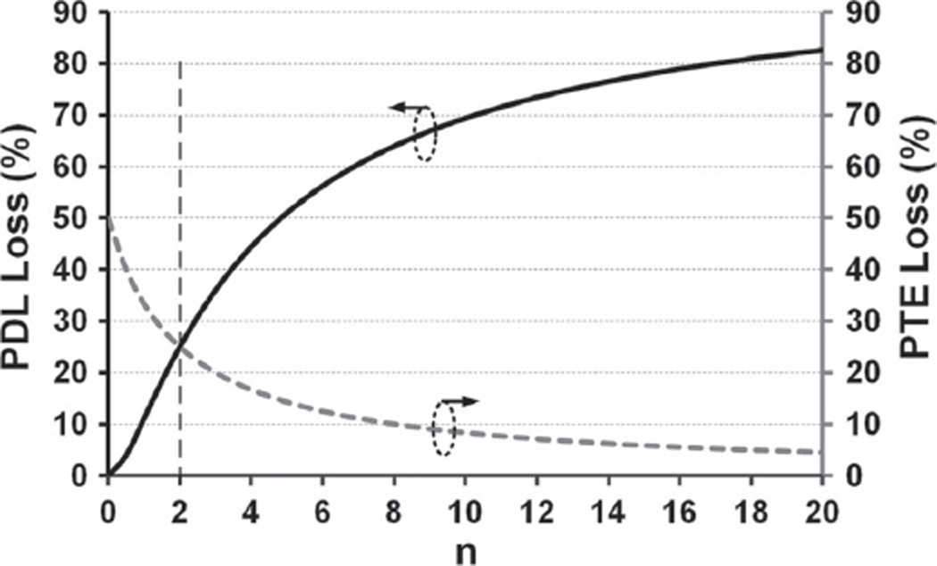
Fig. 2 shows the PTE and PDL losses versus n, based on (9). The key points to be learned from these curves are: 1) If the two-coil link is optimized for the PDL only, i.e., n = 0, it loses 50% of the PTE. 2) If the two-coil link is optimized for the PTE only, i.e., n → ∞, it loses 100% of the PDL. However, in practice, the application and coil fabrication process constraints limit the PTE and allow a small amount of power to be delivered to the load (PDL > 0). 3) When n = 2, the PTE and PDL losses are balanced, equal to 25% each.
Fig. 2.
PTE and PDL losses in percentage with respect to their maximum possible values versus n when the two-coil link is designed to maximize the proposed FoM in (4) as opposed to the PTE or PDL. It can be seen that n = 2 results in similar PTE and PDL losses, equal to 25%. Similar curves can be derived for the three- and four-coil links.
In a particular application, it is often possible to determine whether the PTE, PDL, or both are important. Based on this determination and Fig. 2, the designer can choose a suitable n for the proposed FoM in (4), and proceed with the design of the two-coil link by maximizing it. We believe that n = 2can work well for the majority of applications, in which there is a need to achieve a large PDL with the highest possible PTE, while considering practical driver limitations. Even though in the rest of this paper, we consider n = 2, our discussions are applicable to any desired n in the FoM, defined in (4).
It should also be noted that for a given set of Q2, Q3, and k23 values, there is an optimal load, RL,FoM = ω0L3QL,FoM, which maximizes the FoM of the two-coil link at a particular d23. Calculating the derivative of (5) with respect to QL leads to
| (10) |
Similarly, the optimal load values for PTE and PDL can be calculated from (10) by substituting n with ∞ and 0, respectively [16]
| (11) |
III. Comparison Between Two-Coil Inductive Links Designed Based on Fom, Pte, and Pdl
In this section, we have compared the performance of three different sets of two-coil links, designed based on the PTE, PDL, and the new FoM for IMD applications. First, a design procedure is explained, based on which the optimal coil geometries are calculated. This design procedure will also be used for designing multi-coil links in Section IV. The effects of d23, Rs, and RL, which are often imposed by the application, are studied on the two-coil link design with respect to the FoM.
A. Two-Coil Inductive Link Design Procedure
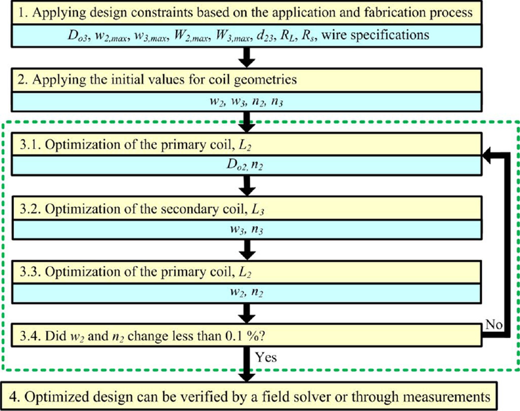
All design examples are based on wire-wound coils (WWC) made of single filament solid wires. The relationship between the inductive link parameters, such as k and Q, and the WWC geometries can be found in the Appendix. The two-coil optimization flowchart in Fig. 3 is similar to the design procedure proposed in [23] with the following differences: 1) WWC geometries are optimized here instead of printed spiral coils (PSCs). In the WWC models presented in the Appendix, the number of turns, ni, in WWCs substitutes the fill factor, Φ, in PSCs while other geometrical parameters remain the same. 2) In Fig. 3, (2), (3), or (5) can be used to maximize the PTE, PDL, or FoM, respectively. Our focus in this paper will be on optimization based on the FoM, while [23] optimizes the PTE. 3) Another difference between Fig. 3 and [23] is that here we have added a weight limit for the coils. This will lead to one more 3-D surface for the weight of the WWC in each step.
Fig. 3.
Iterative two-coil inductive link optimization flowchart.
Fig. 3 starts with the design constraints imposed by the application and coil fabrication technology. The former defines the maximum values for the outer diameter, Do3, of the implantable coil, L3, the maximum wire diameters for L2 and L3, w2,max, w3,max, and their weights, W2,max, W3,max, respectively. For instance, the size and weight of L3 depend on the IMD location in the body. The weight of a circular-shaped WWC with ni turns and a wire spacing of s between the surface of the conductors can be found from (44) in the Appendix. The minimum value for s is twice the thickness of the wire insulation, which is used in the rest of this paper [23]. The nominal values for d23, RL, and Rs are also required in step-1, all determined by the application or initial estimation. The nominal distance, d23, is considered the average spacing between L2 and L3 during normal operation of the inductive link in every particular application.
In step-2, the initial values for L2 and L3 geometries, such as w2, n2, w3, and n3 are chosen. A more detailed discussion about how to choose these initial values can be found in [23]. In step-3.1, key geometrical parameters of L2, i.e., Do2 and n2 are swept, using (5) and (44), respectively, leading to two 3-D surfaces for the FoM and W2. The FoM surface is similar to the PTE surface in [23] when Do2 and Φ2 were swept. Do2 and n2 values that result from the maximum FoM are first chosen. If such values lead to W2 > W2,max, i.e., the resulting optimal coil being too heavy, an imaginary horizontal plane should be drawn over the W2 surface at W2 = W2,max to find the best Do2 and n2 pair on the cross section that give the highest FoM.
Parameters associated with L3 geometry, such as w3 and n3, are swept in step-3.2, using Do2 and n2 values from step-3.1. They generate two 3-D surfaces for FoM and W3 using (5) and (44) in the Appendix. Similar to step-3.1, the FoM surface is similar to the PTE surface in [23] when w3 and Φ3 were swept. The w3 and n3 values that result in the highest FoM and W3 < W3,max are then chosen. In step-3.3, w2 and n2 are swept to maximize the FoM in (5) and still satisfy the W2 < W2,max condition in (44).
Steps 3.1–3.3 are repeated iteratively until w2 and n2 values change < 0.1% from one iteration to the next, satisfying the condition in step-3.4. This step determines the optimal two-coil link geometries that would achieve the maximum FoM. This can be further validated and fine-tuned using field solvers, such as HFSS (Ansoft, Pittsburgh, PA) or through measurements. It should be noted that in steps 3.2 and 3.3, w2 and w3 should be limited to w2,max and w3,max, respectively.
For the IMD design example, we considered a retinal implant with the following assumptions: L2 and L3 were considered circular-shaped WWCs, operating at 13.56 MHz. The link was designed to deliver 250 mW to an RL = 100 Ω from a nominal coupling distance of d23 = 10 mm via a driver (PA) with output resistance of Rs = 0.5 Ω. We also considered Do3 = 10 mm, w3,max = 0.51 mm (AWG24) to reduce the implant thickness, W2,max = 10 g, and W3,max = 0.5 g to limit the weights of L2 and L3 with respect to the electronics [32], [33].
B. PTE versus PDL Tradeoffs
Table I summarizes the results of the design procedure in Fig. 3 for three sets of two-coil inductive links optimized based on the PTE, PDL, and FoM. It can be seen that the link optimized based on the FoM has not only achieved 1.47 times more PTE than the one optimized for PDL (71.3% versus 48.5%) but also provided 16 times larger PDL compared to the one optimized for PTE (180.4 mW versus 11.3 mW for Vs = 1 V). To deliver 250 mW to the load with a class-E PA, driving voltages of Vs = 1.18 V, 4.7 V, and 1.03 V are needed for FoM-, PTE-, and PDL-optimized links, creating peak voltages of 4.2 V, 16.7 V, and 3.7 V across the PA transistor, respectively [31].
TABLE I.
Two-Coil Inductive Link Specifications Results From the PTE-, PDL-, and FoM-Based Optimizations
| Parameters | Symbols | Optimized Parameter | |||
|---|---|---|---|---|---|
| PTE | PDL | FoM | |||
| L2 | Inductance (µH) | L2 | 2.37 | 0.095 | 0.135 |
| Outer diameter (mm) | Do2 | 36 | 13 | 23.2 | |
| Wire diameter (mm) | w2 | 1.15 | 1.2 | 1.75 | |
| Num. of turns | n2 | 10 | 3 | 2 | |
| Wire spacing (µm) | s2 | 100 | |||
| Quality facter* | Q2 | 177.5 | 15.9 | 22.5 | |
| L3 | Inductance (µH) | L3 | 0.024 | ||
| Outer diameter (mm) | Do3 | 10 | |||
| Wire diameter (mm) | w2 | 0.51 | |||
| Num. of turns | n3 | 1 | |||
| Wire spacing (µm) | s3 | 100 | |||
| Quality facter | Q3 | 1248 | |||
| L2–L3 coupling distance (mm) | d23 | 10 | |||
| Max. wire diam. of L2 / L3 (mm) | w2/3,max | − / 0.51 (AWG24) | |||
| Max weight of L2 / L3 (g) | W2/3,max | 10 / 0.5 | |||
| Nominal source resistance (Ω) | RS | 0.5 | |||
| Nominal load (Ω) | RL | 100 | |||
| Power carrier frequancy (MHz) | f0 | 13.56 | |||
| Power transfer efficiency (%) | η | 93.4 | 48.4 | 71.3 | |
| Power delivered to load ** (mW) | PL | 11.3 | 236.7 | 180.4 | |
| Figure-of-Merit (mΩ−1) | FoM | 9.8 | 55.6 | 91.8 | |
Q2 also includes Rs = 0.5 Ω.
Delivered power when Vs = 1 V.
Grayed rows indicate the design constraints.
These results clearly show the disadvantages of the links with low FoM. For instance, the PA for the PTE-optimized link cannot be implemented on-chip in most standard CMOS fabrication processes due to their lower transistor breakdown voltages. On the other hand, the PDL-optimized link, which relaxes the driver design, suffers from low PTE. It should be noted that the FoM-optimized link achieves its high ratings at the cost of only 24% drop in the PTE and PDL compared to the PTE- and PDL-optimized links. This was slightly less than the estimated 25% theoretical level in Fig. 2 due to our WWC fabrication constrains. Hence, unless an application requires very small amount of power, an inductive link that is designed based on the proposed FoM would be preferable by simultaneously providing high PTE and high PDL.
C. Coupling Distance Variations
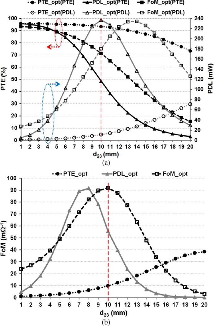
In applications such as IMDs, d23 varies in a wide range, and the inductive link should provide high PTE and PDL for the entire range [34], [35]. Severe misalignments also have a similar effect as increasing d23 by reducing k23. Figs. 4(a) and (b) show the PTE, PDL, and FoM of the links specified in Table I versus d23, respectively. Two important points to be made in these curves are: 1) The PTE and PDL of the PDL-optimized link are significantly reduced at large coupling distances, d23 > 13 mm, while the FoM-optimized link provides both large PTE and PDL, and consequently high FoM, over an extended range. 2) Within smaller coupling distances, d23 < 10 mm, the FoM-optimized link has achieved high PTE and PDL, while the PTE-optimized link suffers from very small PDL. Comparing the FoM of the three sets of links in Fig. 4(b) shows that the link that is optimized based on the proposed FoM maintains the highest performance for a widest range of coupling variations.
Fig. 4.
Comparison between three sets of two-coil links optimized for the PTE, PDL, and FoM versus coupling distance, d23. Rs = 0.5 Ω and RL = 100 Ω. (a) The calculated values of the PTE and PDL for Vs = 1 V (b) The FoM values defined in (4) with n = 2. The inductive links’ specifications for the nominal distance of d23 = 10 mm are summarized in Table I.
D. Source Resistance Effects
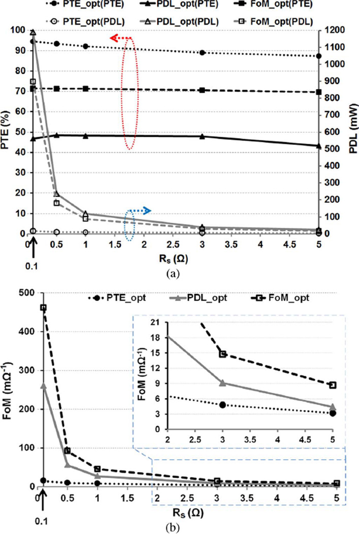
The driver output resistance, Rs, plays an important role in the optimization of the inductive link from the energy source to the load because Rs significantly affects the available power that the PA can deliver through the inductive link [16]. To study the effects of Rs on the two-coil inductive link design, we have optimized our IMD design example for Rs values from 0.1 Ω to 5 Ω. Fig. 5(a) shows that the FoM-optimized link has achieved high PTE and PDL particularly when Rs is small (i.e., when large PDL is needed). For instance, at Rs = 0.1 Ω, the FoM-optimized link has achieved 53 times larger PDL than the PTE-optimized link and only 24.5% less PDL than the PDL-optimized link. On the other hand, the 71.6% PTE of the FoM-optimized link is almost half between the other two designs. As a result, the FoM-optimized link imposes ~7.3 times smaller voltage on the PA transistor compared to the PTE-optimized link for the same amount of PDL. Moreover, Fig. 5(b) shows how the FoM values are higher for the FoM-optimized link versus Rs. For large Rs, which translate to low PDL, the PTE is considered more important, and both PDL and FoM are small for all three links. Therefore, the link designed based on PTE is optimal.
Fig. 5.
Comparison between three sets of two-coil links optimized for PTE, PDL, and FoM versus the driver output resistance, Rs. RL = 100 Ω. (a) The calculated values of the PTE and PDL for Vs = 1V (b) The FoM values defined in (4) for n = 2. The inductive links’ specifications for Rs = 0.5Ω are summarized in Table I.
E. Series versus Parallel Connection of the Load Resistance
Inductive power transmission covers applications with a wide range of power requirements. A common question for designers is whether the secondary loop should be connected in parallel, similar to Fig. 1, or in series (as in Fig. 7). In [28], the loaded quality factor of the secondary loop, Q3L, which only depends on the L3 geometry and RL, has been used to differentiate between parallel and series load connections. In [36], however, it is shown that the series or parallel load connection also depends on k23 and whether the link should be optimized for the PTE or PDL. Overall, the indication between whether the secondary loop should be connected in series or in parallel is not very clear.
Fig. 7.
Lumped circuit model of a three-coil inductive power transmission link with the PA loss modeled as Rs.
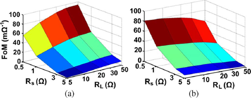
The proposed FoM can clearly determine the superior secondary loop topology, while considering both PTE and PDL, which are already linked to k23 and coils geometries. We optimized our IMD design example based on the FoM for different RL and Rs values for parallel and series secondary configurations and depicted the results in Fig. 6(a) and (b), respectively. All equations in Section II are applicable for the series topology, except for QL, which should be defined as ω0L3/RL. It can be seen that for RL < 10 Ω, the series connection results in higher FoM, almost regardless of Rs, while for larger RL, the parallel connection is superior. Therefore, for the IMDs, in which RL is often larger than 10 Ω, the parallel secondary configuration is preferred.
Fig. 6.
The FoM comparison for parallel and series load connection versus RL and Rs: (a) Parallel load connection. (b) Series load connection. The inductive links specifications are summarized in Table I.
IV. Multi-Coil Inductive Power Transmission Links
Multi-coil inductive power transmission in the form of three-and four-coil links has been proposed based on the coupled mode theory to achieve high PTE particularly at large distances [26], [37]. We have also presented a comprehensive circuit-based analysis of multi-coil links in [16] and [38]. However, the optimal choice between the two-, three-, and four-coil links for a particular application is yet another source of confusion for designers, which can be addressed by our proposed FoM.
In an m-coil link, the reflected load from the (i + 1)th coil to the ith coil can be found from [16],
| (12) |
where ki,i+1 is the coupling coefficient between the ith and (i + 1)th coils. Q(i+1)L is the loaded quality factor of the (i + 1)th coil, which can be found from
| (13) |
where Qi = ωLi/Ri and Ri are the unloaded quality factor and parasitic series resistance of the ith coil (Li), respectively. It should be noted that for the last coil, which is connected to the load in series, QmL = ωLm/(Rm + RL) and for the first coil, which is connected to the source in series, Rs should be added to R1.
Assuming that the coupling between non-neighboring coils is negligible, the partial PTE from the ith coil to (i + 1)th coil can be written as
| (14) |
Using (12)–(14), the overall PTE in such a multi-coil inductive link can be found from
| (15) |
PDL can be calculated by multiplying the power provided by the source, i.e., , by the PTE from (15)
| (16) |
A. Three-Coil Inductive Power Transmission Link
The three-coil inductive power transmission link, shown in Fig. 7, can be used to achieve high PTE and PDL by adjusting k34 to transform any arbitrary RL into the optimal resistance required in the L2 − L3 inductive link [16]. The PTE of this circuit can be calculated by reflecting the resistive components of each loop from the load back toward the primary coil loop, one stage at a time, using (12), and calculating the percentage of the power that is delivered from one stage to the next, using (14), until it reaches RL. According to (15), this leads to [16]
| (17) |
where k24 has been ignored due to the large separation between L2 and L4. One can also calculate the PDL of this circuit using (12)–(16)
| (18) |
It should be noted that in (17) and (18), the driver output resistance should be considered in Q2 = ωL2/(R2 + Rs) [16].
The FoM for a three-coil inductive link can be found by substituting (17) and (18) in (4)
| (19) |
It will be shown that, similar to two-coil links, the PTE and PDL losses in three-coil links follow Fig. 2 and (9), when optimized for the FoM in (4) and (19).
The PTE profile of the three-coil link according to (17) is a monotonically decreasing function of the coils’ coupling distance, d23 [16]. However, the PDL and FoM profiles are maximized at a particular d23 that can be found by calculating the derivatives of (18) and (19) versus k23, respectively
| (20) |
By substituting k23,FoM in (17) and (18), one can find the PTE and PDL of the three-coil link when it is designed to maximize the FoM at that particular d23
| (21) |
Additional constraints on the coils’ geometries in order to satisfy the application or fabrication requirements may result in further reductions in the PTE and/or PDL. The maximum achievable PTE and PDL at a particular d23 can be calculated from (21) by substituting n with ∞ and 0, respectively
| (22) |
Using (21) and (22), we can calculate the losses in PTE and PDL when the link is designed based on the optimal FoM
| (23) |
The results are exactly the same as those found in (9) for the two-coil links. It should be noted that in comparison to two-coil links, the three-coil inductive links have an additional degree of freedom owing to k34, which allows them to transform any arbitrary RL to the optimal values for FoM, PTE, and PDL in (10) and (11). Two-coil links fail to achieve the optimal QLs in (10) and (11), which become quite large when k23 drops as a result of large d23 or severe misalignments [16].
B. Four-Coil Inductive Power Transmission Links
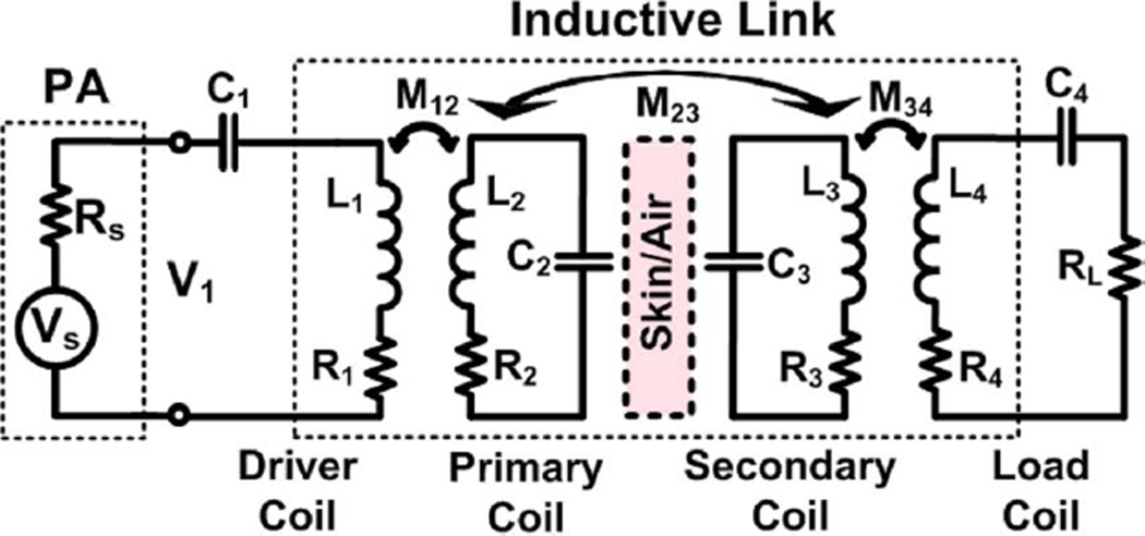
Fig. 8 shows a four-coil inductive power transmission link, which is capable of achieving a high PTE by adjusting k12 when there is a large Rs, imposed by a weak driver. In four-coil inductive links, there is a tradeoff between the highest PTE that can be achieved at short distances while maintaining sufficient PDL at large distances [16]. The PTE of the four-coil link can be calculated using (12)–(15)
| (24) |
| (25) |
where k13, k14, and k24 are ignored in comparison to k12, k23, and k34. Using (14)–(16), PDL of the four-coil inductive links can be found from
| (26) |
It should be noted that in (24)–(26), the driver output resistance should be considered in Q1 = ωL1/(R1 + Rs).
Fig. 8.
Lumped circuit model of the four-coil inductive power transmission link with the PA loss modeled as Rs.
The four-coil FoM can be calculated by substituting (24) and (26) in (4)
| (27) |
| (28) |
The four-coil PTE, PDL, and FoM profiles are maximized at a particular d23 that can be found by calculating the derivatives of (24), (25), and (27) with respect to k23, respectively, as shown by (28) at the bottom of the page.
The optimal k23,FoM in (28) is too complicated to be used for calculating the PTE and PDL losses as a result of FoM-based optimization. Therefore, we apply some approximation. In four-coil links, we know that k12 should be large in order to achieve a high PTE between L1 and L2(η12 ≈ 1), particularly at short coupling distances where L2 is strongly loaded by L3 [16]. Assuming , we can conclude that in (25), B ≫ A. Therefore, k23,FoM in (28) can be further simplified to
| (29) |
By substituting k23,FoM in (24) and (26), and assuming B ≫ A, one can find the PTE and PDL of the four-coil link when the FoM is maximized at a particular d23
| (30) |
The maximum achievable PTE and PDL at a particular d23 are calculated by substituting n with ∞ and 0, respectively
| (31) |
Using (30) and (31), similar to the two- and three-coil links, we can calculate the losses in PTE and PDL when the four-coil link is designed based on the optimal FoM
| (32) |
Interestingly, the results are consistent with those found in (9) and (23). Therefore, designers can use the PTE and PDL loss curves in Fig. 2 to find the best n for a given application.
C. Design Procedure for Multi-Coil Power Transmission Links Based on the Proposed FoM
In Section III, we presented an iterative optimization procedure for two-coil inductive links based on the new FoM, which has been extended for multi-coil links. The relationship between the inductive link parameters, such as k and Q, and the WWC geometries can be found in the Appendix.
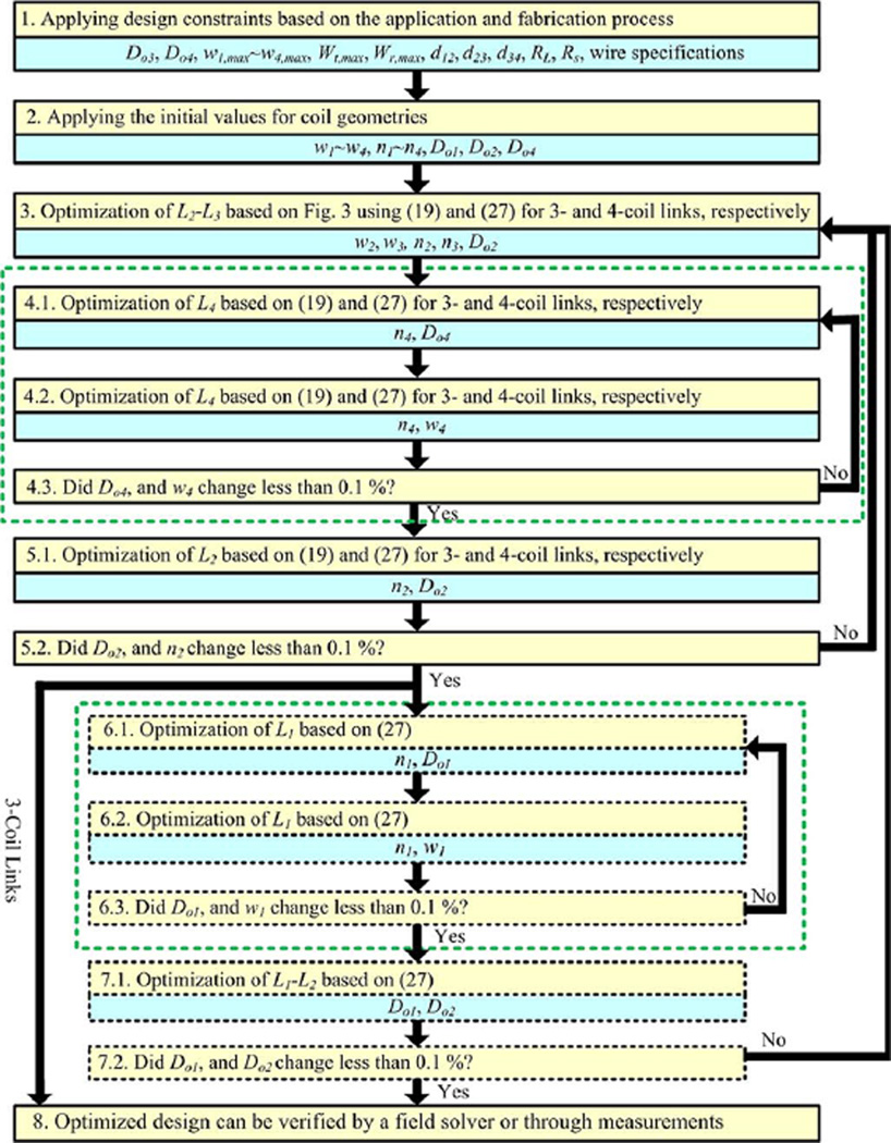
In step-1 of Fig. 9 flowchart, the design constraints imposed by the application and coil fabrication technology are applied. Using (44) in the Appendix, the weight of the coils on the Tx side, Wt, is defined as the weight of L2 or the sum of the weights of L1 and L2 for three- and four-coil links, respectively. The weight of the Rx coils, Wr, also equals the sum of the weights of L3 and L4 for both three- and four-coil links. The nominal values for Do3, d12, d23, d34, RL, and Rs are also required in this step, which are defined by the application (d12 is needed only for the four-coil link). Do3 is often chosen to be the maximum allowed by the application, particularly in IMDs. The designer should also limit the coils’ wire diameters, w1,max ~ w4,max, to account for the overall thickness of the inductors in the given application. The minimum wire spacing between the surface of the conductors, s1 ~ s4, is considered twice the thickness of the wire insulation in all WWCs [23].
Fig. 9.
Iterative multi-coil links optimization flowchart based on the proposed FoM.
In step-2, the initial values for L1 ~ L4 geometries namely w1 ~ w4, n1 ~ n4, Do1, Do2, and Do4 are chosen. In step-3, L2 − L3 link is optimized using the design procedure shown in Fig. 3, with (19) and (27) used instead of (5) for three- and four-coil links, respectively. This step provides the interim optimal values for w2, w3, n2, n3, and Do2 based on the initial values for L1 and L4 geometries.
L4 geometry is optimized in step-4 by sweeping n4 and Do4, followed by sweeping n4 and w4 using (19) and (27) for three-and four-coil links, respectively. In each step, two 3-D surfaces for FoM and Wr are obtained while n4 and Do4 or n4 and w4 values that result in the maximum FoM and Wr < Wr,max are chosen. Steps 4.1 and 4.2 are repeated iteratively until Do4 and w4 change less than 0.1% and satisfy the condition in step-4.3.
In step-5, key parameters in the geometry of L2, i.e., n2 and Do2, are swept to maximize the FoM in (19) and (27) for three- and four-coil links, respectively, while maintaining Wt < Wt,max. Step-5 also verifies whether the L4 geometry resulted from step-4 is optimal. This is because L4 was optimized in step-4 with respect to L3 to achieve the desired k34 while L2 − L3 link had been optimized in step-3 with non-optimized L1 and L4 geometries. Steps-3 and 4 are repeated iteratively until n2 and Do2 change less than 0.1%, and satisfy the condition in step-4.3. This step concludes the three-coil link design for maximum FoM, which can be further validated using field solvers, such as HFSS (Ansoft, Pittsburgh, PA).
The rest of steps in Fig. 9 are specific to four-coil links to optimize the geometry of L1 for the highest FoM based on (27). Step-6 is similar to step-4, which determines the optimal geometry of L1. However, step-7 verifies if the L2 geometry is still optimal for the new L1 geometry from step-6. Therefore, Do1 and Do2 are swept in step-7.1 to maximize FoM in (27) while keeping Wt < Wt,max. The new Do1 along with n1 and w1 from step-6.2 are used to start a new iterative optimization loop from step-3, as long as Do1 and Do2 change more than 0.1% in step-7.2. The four-coil link is designed for maximum FoM if the condition in step-7.2 is satisfied.
V. Inductive Power Transmission Links for Industrial Applications
Recharging HMDs and EVs need high PDLs in the order of watts to kilowatts. In this section, we have provided design examples for industrial applications to differentiate between the two-, three-, and four-coil links based on our proposed FoM.
A. Wireless Charging of HMDs
Wireless chargers for transferring energy over several tens of cm to charge HMDs or operate small home appliances are now commercially available [39]. Here, we have designed three sets of inductive links for HMD charging application with two, three, and four WWCs. These links were designed based on our proposed FoM optimization procedure in Fig. 9, and the results are summarized in Table II. These links operate at 13.56 MHz and deliver 1.6 W to an RL = 5 Ω from a nominal coupling distance of d23 = 10 cm using a PA with Rs = 0.5 Ω. The maximum wire diameters of L3 and L4, w3,max and w4,max, were considered to be 0.64 mm (AWG22), while L1 and L2 maximum wire diameters, w1,max and w2,max, were limited to 1.6 mm (AWG14) to reduce the Tx and Rx size and thickness. Furthermore, in order to shrink the size of the Rx module, Do3 was limited to 4 cm, and L4 in the three- and four-coil links was placed in the middle of L3. Similarly, L1 in the four-coil link was placed in the middle of L2. It should be noted that according to Section III-E, the secondary loop for the two-coil link was connected in series because of the small RL value.
TABLE II.
Multi-Coil Inductive Link Specifications for the FoM-Based Optimization for HMD Charging Application
| Parameters | Symbols | 2-coil | 3-coil | 4-coil | |
|---|---|---|---|---|---|
| L1 | Inductance (µH) | L1 | - | - | 0.21 |
| Outer diameter (cm) | Do1 | - | - | 3 | |
| Wire diameter (mm) | w1 | - | - | 1.6 | |
| Num. of turns | n1 | - | - | 2 | |
| Wire spacing (µm) | s1 | - | - | 100 | |
| Quality factor* | Q1 | - | - | 34.6 | |
| L2 | Inductance (µH) | L2 | 1.4 | 1.3 | 0.52 |
| Outer diameter (cm) | Do2 | 12.5 | 11.7 | 15 | |
| Wire diameter (mm) | w2 | 1.6 | |||
| Num. of turns | n2 | 2 | 2 | 1 | |
| Wire spacing (µm) | s2 | 100 | |||
| Quality factor* | Q2 | 116.8 | 117.5 | 427 | |
| L3 | Inductance (µH) | L3 | 4.6 | 0.13 | |
| Outer diameter (cm) | Do3 | 4 | |||
| Wire diameter (mm) | w3 | 0.64 | |||
| Num. of turns | n3 | 9 | 1 | ||
| Wire spacing (µm) | s3 | 100 | |||
| Quality factor | Q3 | 222.8 | 553.3 | ||
| L4 | Inductance (nH) | L4 | - | 40.8 | 42.4 |
| Outer diameter (cm) | Do4 | - | 1.6 | 1.65 | |
| Wire diameter (mm) | w4 | - | 0.64 | ||
| Num. of turns | n4 | - | 1 | ||
| Wire spacing (µm) | s4 | - | 100 | ||
| Quality factor | Q4 | - | 1092 | 1068 | |
| L2 and L3 coupling distance (cm) | d23 | 10 | |||
| Max. wire diam. of Tx coils (mm) | w1/2,max | 1.6(AWG14) | |||
| Max. wire diam. of Rx coils (mm) | w3/4,max | 0.64(AWG22) | |||
| Nominal source resistance (Ω) | RS | 0.5 | |||
| Nominal load (Ω) | RL | 5 | |||
| Power carrier frequency (MHz) | f0 | 13.56 | |||
| Power transfer efficiency (%) | η | 28.4 | 36.1 | 42.8 | |
| Power delivery to load** (mW) | PDL | 79 | 92 | 14.4 | |
| Figure-of-Merit (mΩ−1) | FoM | 6.4 | 12 | 20.9 | |
Q1 in 4-coil and Q2 in 2- and 3-coil links also include Rs = 0.5 Ω.
Delivered power when Vs = 1 V
Grayed rows indicate the design constraints.
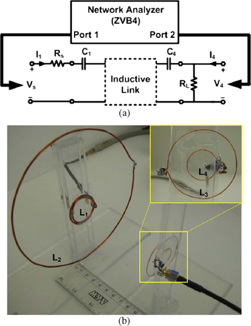
Fig. 10(a) shows the setup, proposed in [16], to accurately measure the PTE and PDL of a multi-coil inductive link. The FoMs are then calculated from the measured PTE and PDL values using (4) with n = 2. In this method, resonance capacitors, Rs, and RL in Figs. 1(a), 7, and 8 for two-, three-, and four-coil links, respectively, are all connected to the coils, which are collectively considered a two-port system along with the multi-coil inductive link. The network analyzer is then used to measure the S-parameters and consequently the Z-parameters [40]. The PTE and PDL are found from the two-port equations
| (33) |
where Z11 = V1/I1 and Z41 = V4/I1 are measured when I4 = 0, with the acceptable assumption that the network analyzer loading of the inductive link is negligible compared to RL.
Fig. 10.
(a) The PTE and PDL measurement setup using network analyzer with all the coils tuned at the carrier frequency, and both Rs and RL connected in the setup, (b) Four-coil inductive link used to measure the PTE and PDL. Coil specifications are listed in Table II.
Fig. 10(b) shows the experimental setup for measuring the PTE and PDL in a four-coil inductive link. These coils were fabricated based on the values listed in Table II and held in parallel and perfectly aligned using Plexiglas supports. L1 and L4 were placed in the middle of L2 and L3 in a co-planar and co-centric fashion to achieve k12 = 0.03 and k34 = 0.092, respectively, in the four-coil link. In the three-coil link, k34 = 0.088 when L4 is placed in the middle of L3.
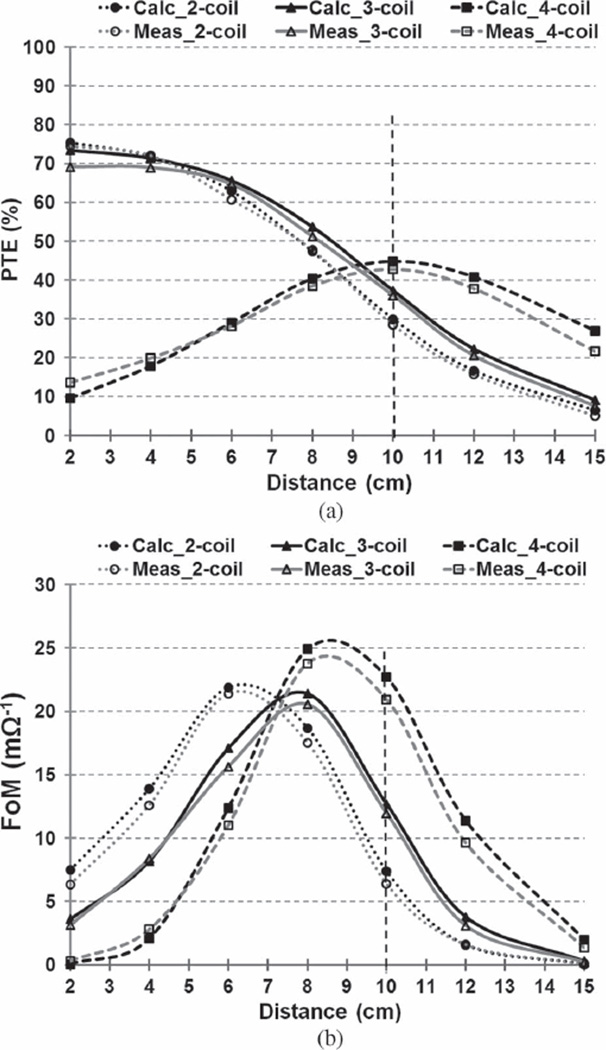
Fig. 11(a) and (b) show the differences between calculated and measured values of the PTE and FoM, respectively, for the two-, three-, and four-coil links. It can be seen in Fig. 11(a) that the four-coil link PTE (42.8%) is higher than the two- and three-coil link PTEs (28.4% and 36.1%, respectively) for d23 ≥ 9.5 cm. According to Fig. 11(b), the four-coil link has also achieved higher FoM (20.9 mΩ−1) compared to its two- and three-coil counterparts (6.4 mΩ−1 and 12 mΩ−1, respectively) for d23 ≥ 7.5 cm. However, this superior FoM at d23 = 10 cm, which is the nominal distance for this design, comes at the cost of much lower PTE, and consequently the FoM, at shorter coupling distances, as shown in Fig. 11(a) and (b). This is because the PDL of the four-coil link has been deliberately increased at d23 = 10 cm by reducing k12 (by reducing Do1) to maximize the FoM. The PTE and FoM drop at short distances confirm our conclusion in [16] that there is an inherent tradeoff between achieving high PDL at larger distances with a high PTE at smaller distances in four-coil links.
Fig. 11.
Comparison between measured and calculated values of the (a) PTE, and (b) our proposed FoM versus coupling distance, d23 for two-, three-, and four-coil inductive links specified in Table II for HMD applications (Vs = 1 V).
However, the three-coil link has achieved both high PTE and FoM at both large and small distances. Based on the PDL values in Table II for Vs = 1 V, to deliver 1.6 W to the load with a class-E PA, the two-, three-, and four-coil links need Vs = 4.5 V, 4.2 V, and 3.7 V and peak voltages across the PA transistor of 16 V, 15 V, and 13.2 V, respectively. These voltage levels are reasonable thanks to the use of FoM. However, they could be much larger if PTE had been optimized instead.
Small discrepancies between the calculated and measured PTEs are due to the measurement non-idealities and limited Q of the tuning capacitors, which have been considered ideal in our models. The capacitors’ measured Q was < 5000 at 13.56 MHz, which can reduce the unloaded Q3 in three-coil and Q2 and Q3 in four-coil links by 10%. The FoM curves show more error because the PTE and PDL errors accumulate in the FoM = η2 × PL(Vs = 1 V).
B. Wireless Charging of EVs
We have designed two-, three-, and four-coil inductive links, using WWCs, for the EV charging application based on the proposed FoM guideline. Table III summarizes the results of the optimization procedure in Fig. 9. These links operate at 145 kHz and deliver 3.3 kW to an RL = 20 Ω from a nominal coupling distance of d23 = 20 cm using a PA driver with 0.5 Ω output resistance. The thicknesses of the Tx and Rx circular-shaped WWCs, i.e., w1,max, w2,max, w3,max, and w4,max, were limited to 5 cm to reduce the size of the charger inductors. L3 diameter, Do3, was also limited to 50 cm to easily fit under different vehicles. Furthermore, L4 in the three- and four-coil links and L1 in the four-coil link were placed in the middle of L3 and L2, respectively, leading to d34 = d12 = 0 mm. The secondary loop for the two-coil link was connected in series to achieve higher FoM, based on our calculations.
TABLE III.
Multi-Coil Inductive Link Specifications for the FoM-Based Optimization for EV Charging Application
| Parameters | Symbols | 2-coil | 3-coil | 4-coil | |
|---|---|---|---|---|---|
| L1 | Inductance (µH) | L1 | - | - | 1.66 |
| Outer diameter (cm) | Do1 | - | - | 14 | |
| Wire diameter (mm) | w1 | - | - | 7.7 | |
| Num. of turns | n1 | - | - | 3 | |
| Wire spacing (µm) | s1 | - | - | 100 | |
| Quality factor* | Q1 | - | - | 2.9 | |
| L2 | Inductance (µH) | L2 | 11.8 | 5.4 | 1.11 |
| Outer diameter (cm) | Do2 | 75 | 62 | 34.3 | |
| Wire diameter (mm) | w2 | 45 | 50 | 50 | |
| Num. of turns | n2 | 4 | 3 | 2 | |
| Wire spacing (µm) | s2 | 100 | |||
| Quality factor* | Q2 | 18.1 | 9.3 | 209.2 | |
| L3 | Inductance (µH) | L3 | 62.6 | 5 | 4.9 |
| Outer diameter (cm) | Do3 | 50 | |||
| Wire diameter (mm) | w3 | 10.3 | 35 | 45 | |
| Num. of turns | n3 | 11 | 3 | 4 | |
| Wire spacing (µm) | s3 | 100 | |||
| Quality factor | Q3 | 39 | 138.9 | 116 | |
| L4 | Inductance (µH) | L4 | - | 3.97 | 6.3 |
| Outer diameter (cm) | Do4 | - | 45 | 34 | |
| Wire diameter (mm) | w4 | - | 12.6 | 17 | |
| Num. of turns | n4 | - | 2 | 4 | |
| Wire spacing (µm) | s4 | - | 100 | ||
| Quality factor | Q4 | - | 94.1 | 101 | |
| L2 and L3 coupling distance (cm) | d23 | 20 | |||
| Max. wire diam. of Tx coils (mm) | w1/2,max | 50 | |||
| Max. wire diam. of Rx coils (mm) | w3/4,max | 50 | |||
| Nominal source resistance (Ω) | RS | 0.5 | |||
| Nominal load (Ω) | RL | 20 | |||
| Power carrier frequency (kHz) | f0 | 145 | |||
| Power transfer efficiency (%) | η | 60.8 | 69.3 | 66.7 | |
| Power delivery to load** (mW) | PDL | 176.4 | 169.3 | 163 | |
| Figure-of-Merit (mΩ−1) | FoM | 65.3 | 81.3 | 72.6 | |
Q1 in 4-coil and Q2 in 2- and 3-coil links also include Rs = 0.5 Ω.
Delivered power when Vs = 1 V
Grayed rows indicate the design constraints.
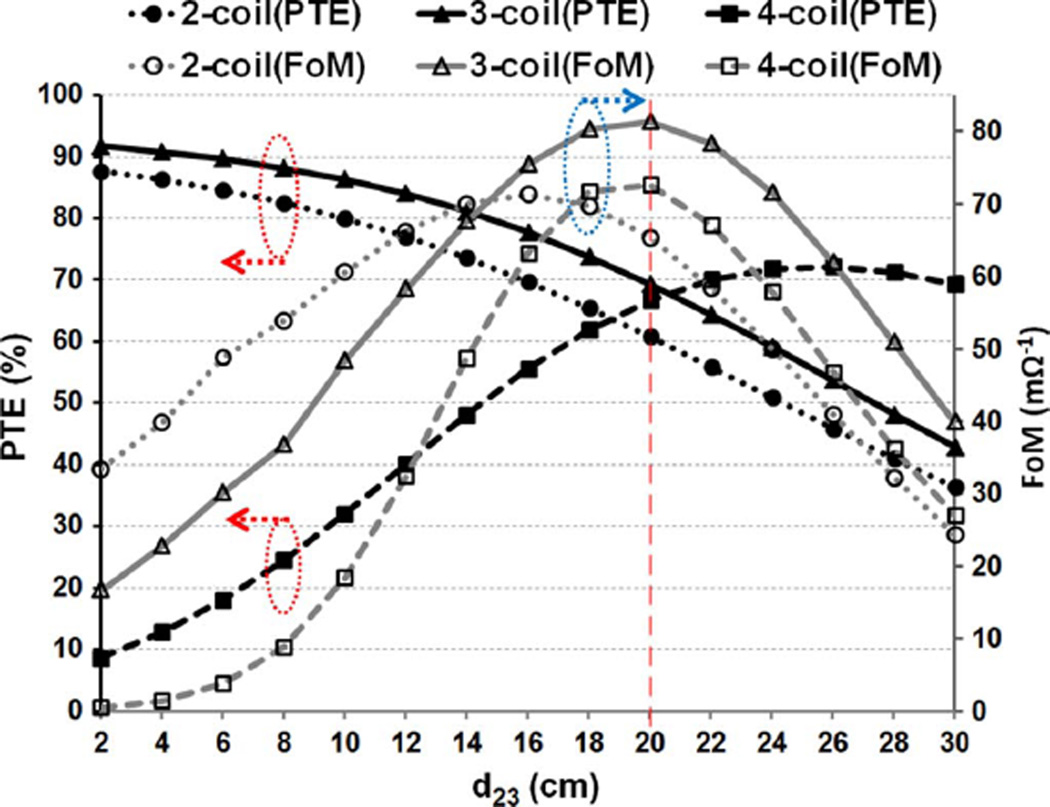
Fig. 12 shows the comparison between the calculated PTE and FoM values in two-, three-, and four-coil inductive links. It can be seen that at d23 = 20 cm, the three-coil link has achieved larger FoM (81.3 mΩ−1) compared to its four- and two-coil counterparts (72.6 mΩ−1 and 65.3 mΩ−1, respectively). According to Fig. 12, the four-coil link not only achieves lower PTE and FoM than the three-coil link at d23 = 20 cm but also shows inferior performance at smaller d23. The two-coil link performance is comparable to three-coil and even better in terms of PTE at lower d23 because L2 and L3 are strongly coupled (k23 = 0.2) and achieving QL,FoM in (10) for the two-coil link is feasible.
Fig. 12.
Comparison between calculated values of PTE and FoM versus d23 for two-, three-, and four-coil inductive links for wireless EVs charging applications specified in Table III (Vs = 1 V).
In a class-C PA, optimal design allows for high-power efficiency with peak voltages across the primary coil and the PA transistor that are close to VDD and 2VDD, respectively [31]. Based on the PDL values in Table III for Vs = 1 V, in order to deliver 3.3 kW to the load with a class-C PA, the two-, three-, and four-coil links will need Vs = 137 V, 140 V, and 142 V, resulting in 274 V, 280 V, and 284 V peak voltages across the PA transistor, respectively. It should be noted that these voltage levels would have been much larger, and therefore impractical, if the links had been optimized based on the PTE.
Metallic objects around the inductive link, particularly in EV applications, can affect the inductive link performance. The geometries and relative positioning of such metallic objects can be entered in field solvers, such as HFSS, to account for phenomena such as the eddy current. Furthermore, ferrite cores can be used to increase the mutual coupling between the coils and potentially improve the FoM. However, modeling, design, and optimization of the ferrite cores are out of the scope of this paper [44].
VI. Discussion
There are a number of parameters that can guide designers toward the optimal inductive power transmission link for their specific application. The amount of PDL (PL), driver output resistance (Rs), source voltage (Vs), nominal coupling distance (d23), and the range of coupling distance variations or coil misalignments are among important parameters in addition to the application-based limitations on the coils geometries. The optimization procedure can be made much simpler if it can be shaped around a single measure that would best fit the application. PTE, which has been dominantly used in the past, is a good measure when PL is small or Rs is large. However, delivering sufficient PDL becomes challenging when there are stringent limitations on the PA driver. Hence, for the majority of applications, in which achieving high PTE and PDL are both important, our proposed FoM would be a better choice.
Another challenge for designers is how to choose between different topologies, i.e., two-, three-, and four-coil links, for their given application. As demonstrated, three examples across a wide range of power levels, most often the proposed FoM can clearly show the topology that fits the best. If two different topologies achieve similar or close FoMs, one can change the parameter n in (4) to give a heavier weight to PTE (higher) or PDL (lower). Our recommendation is going for a higher PTE because the necessary PDL can be achieved by increasing Vs, as long as the PA transistors can handle the higher voltage levels. According to earlier design examples, the two-, three-, and four-coil links are suitable for these conditions: 1) Two-coil links are chosen when the coils are strongly coupled, and a large PDL is needed, i.e., Rs is small. This is because the optimal QLs for FoM, PTE, and PDL in (10) and (11) are easier to achieve with a large k23. Another justification for using a two-coil link is extreme size constraints. 2) Three-coil links are chosen when the coils are loosely coupled, the coupling distance varies in a wide range, and a large PDL is needed. 3) Finally, four-coil links are optimal when the PTE is paramount, the load power consumption is very small, the coils are loosely coupled, and their relative distance and alignment are stable.
In high-power applications, Rs mainly represents the large signal resistance of the driver, which would change with the voltage swing around the driver transistor, temperature, and frequency of operation. Therefore, the largest possible Rs was chosen for the inductive link design to achieve the highest FoM in the worst case condition. Rs variations change the PDL according to (3), (18), and (26) for two-, three-, and four-coil inductive links, respectively, and if necessary, can be compensated by a closed-loop power transmission mechanism [34].
The additional degree of freedom provided by k34 in three-coil links and k34 and k12 in four-coil links allows designers to increase the loaded quality factor of L3 (Q3L) and L2 (Q2L in four-coil links). This leads to higher sensitivity to carrier frequency variations or detuning in multi-coil links, resulting in considerable degradation in both PTE and PDL. There is little concern about detuning of L4 and L1 because these coils have very small loaded quality factors and therefore are much less sensitive to frequency shifts.
VII. Conclusion
A new FoM has been proposed to design high-performance inductive power transmission links. We have demonstrated the tradeoffs between maximizing the PTE and PDL, simultaneously, to help designers choose the best measure for a particular application. It is even possible to tune the FoM to give more weight to PTE over PDL or vice versa. We have proposed a design procedure based on the new FoM for two-coil links and extended it to multi-coil arrangements for designing state-of-the-art inductive power transmission links. Three design examples, ranging from milliwatt to kilowatt power levels, were presented to show the usage and efficacy of the proposed FoM, which can also differentiate between two-, three-, and four-coil inductive links for a given application. The FoM guides designers to choose two-coil links for strongly coupled coils used in applications that need large PDL, three-coil links for loosely coupled coils where the coupling distance varies considerably, and four-coil links when small PDL is required at high PTE and the coils are loosely coupled but have a stable coupling distance and alignment.
ACKNOWLEDGMENT
The authors would like to thank Uei-Ming Jow for his help with the modeling and measurements.
This work was supported in part by the National Institutes of Health under Grant NIBIB-1R21EB009437-01A1 and Grant NINDS-1R01NS062031-01A1, and in part by National Science Foundation Award ECCS-824199.
Biographies

Mehdi Kiani (S’09) received the B.S. degree from Shiraz University, Shiraz, Iran, and the M.S. degree from Sharif University of Technology, Tehran, Iran, in 2005 and 2008, respectively. He joined the GT-Bionics Laboratory at the Georgia Institute of Technology, Atlanta, in 2009, where he is working toward the Ph.D. degree.

Maysam Ghovanloo (S’00–M’04–SM’10) was born in 1973 in Tehran, Iran. He received the B.S. degree in electrical engineering from the University of Tehran, Tehran, in 1994, the M.S. degree in biomedical engineering from the Amirkabir University of Technology, Tehran, in 1997, and the M.S. and Ph.D. degrees in electrical engineering from the University of Michigan, Ann Arbor, in 2003 and 2004, respectively.
From 2004 to 2007, he was an Assistant Professor in the Department of Electrical and Computer Engineering, North Carolina State University, Raleigh. In 2007, he joined the faculty of Georgia Institute of Technology, Atlanta, where he is currently an Associate Professor and the Founding Director of the GT-Bionics Laboratory in the School of Electrical and Computer Engineering. He has authored or coauthored more than 100 peer-reviewed publications.
Dr. Ghovanloo is a member of the IEEE Solid-State Circuits, IEEE Circuits and Systems, and IEEE Engineering in Medicine and Biology Societies and of the American Association for the Advancement of Science. He is a member of the Imagers, MEMS, Medical, and Displays Subcommittee of the International Solid-State Circuits Conference. He has organized several special sessions and was a member of Technical Review Committees for major conferences in the areas of circuits, systems, sensors, and biomedical engineering. He is an Associate Editor of the IEEE Transactions on Biomedical Engineering and the IEEE Transactions on Biomedical Circuits and Systems. He was the 2010 recipient of a CAREER award from the National Science Foundation. He is also a member of Tau Beta Pi and Sigma Xi.
Appendix
WWCs are often modeled as distributed RLC networks with a self-inductance in series with a resistance, both of which are in parallel with the coil parasitic capacitance [41]. An analytical expression for the self-inductance of a one turn circular conductive loop can be found from [41]
| (34) |
where μ0 and μr are the permeability of space and of the conductor, respectively. Do is the diameter of the loop, and w is the diameter of the wire. For mutual inductance, M, a WWC can be considered a set of concentric single-turn loops with various diameters, all connected in series. Using Maxwell equations, Mij between a pair of parallel single-turn circular loops at radii ri = Di/2 and rj = Dj/2 can be found from [23]
| (35) |
where
| (36) |
In this equation, dij is the coupling distance between the two coils and i ≠ j. K(α) and E(α) are the complete elliptic integrals of the first and second kind, respectively [23]. Therefore, the mutual inductance between two coils with ni and nj number of turns can be found from
| (37) |
Hence, the self-inductance of a WWC can be found from
| (38) |
To model the series parasitic resistance of the WWC, its dc resistance should be calculated from
| (39) |
where ρc is the resistivity of the conductive material, s is the wire spacing between the surface of the conductors, and ni is ith coil total number of turns. As the operating frequency increases, the skin effect increases the series resistance, which can be modeled as [43]
| (40) |
where
| (41) |
When the wire spacing, s, is smaller than the wire diameter, w, the ac resistance of the coil in (40) increases due to the proximity effect at higher frequencies [45].
The parasitic capacitance between two turns of a WWC can be found from [41]
| (42) |
where εr is the relative permittivity of the insulation material, ς is the thickness of the insulation layer, θe is the effective angle between turn i and turn j, i.e., 90°, and s′ is the wire spacing between the surface of the insulation layers. Hence, the sum of the turn-to-turn parasitic capacitance from (42) leads to the total parasitic capacitance, CP.
Finally, considering RS in series with Lself and CP in parallel with both, the quality factor of a WWC at operating frequency, ω0, can be found from [23]
| (43) |
which is valid for low frequency and small CP.
The weight of a circular-shaped WWC with ni turns, wire spacing of s between the surface of the conductors, and wire diameter of w can be written as
| (44) |
where ρ is the density of the conducting material, which is 8.96 g/cm3 for copper. In (44), we have ignored the weight of the insulating material.
Footnotes
Color versions of one or more of the figures in this paper are available online at http://ieeexplore.ieee.org.
Contributor Information
Mehdi Kiani, Email: m_kiani@gatech.edu.
Maysam Ghovanloo, Email: mgh@gatech.edu.
References
- 1.Finkenzeller K. RFID-Handbook. 2nd ed. Hoboken, NJ: Wiley; 2003. [Google Scholar]
- 2.Chen SCQ, Thomas V. Optimization of inductive RFID technology; Proc. IEEE Int. Symp. Electron. Environ; 2001. May, pp. 82–87. [Google Scholar]
- 3.Clark GM. Cochlear Implants: Fundamentals and Applications. New York: Springer-Verlag; 2003. [Google Scholar]
- 4.Chen K, Yang Z, Hoang L, Weiland J, Humayun M, Liu W. An integrated 256-channel epiretinal prosthesis. IEEE J. Solid-State Circuits. 2010 Sep;45(no. 9):1946–1956. [Google Scholar]
- 5.Harrison RR, Watkins PT, Kier RJ, Lovejoy RO, Black DJ, Greger B, Solzbacher F. A low-power integrated circuit for a wireless 100-electrode neural recording system. IEEE J. Solid-State Circuits. 2007 Jan;42(no. 1):123–133. [Google Scholar]
- 6.Hirai J, Kim TW, Kawamura A. Study on intelligent battery charging using inductive transmission of power and information. IEEE Trans. Power Electron. 2000 Mar;15(no. 2):335–345. [Google Scholar]
- 7.Kim C, Seo D, You J, Park J, Cho B. Design of a contactless battery charger for cellular phone. IEEE Trans. Ind. Electron. 2001 Dec;48(no. 6):1238–1247. [Google Scholar]
- 8.Hatanaka K, Sato F, Matsuki H, Kikuchi S, Murakami J, Kawase M, Satoh T. Power transmission of a desk with a cord-free power supply. IEEE Trans. Magn. 2002 Sep;38(no. 5):3329–3331. [Google Scholar]
- 9.Jang Y, Jovanovic MM. A contactless electrical energy transmission system for portable-telephone battery chargers. IEEE Trans. Ind. Electron. 2003 Jun;50(no. 3):520–527. [Google Scholar]
- 10.Hui S, Ho W. A new generation of universal contactless battery charging platform for portable consumer electronic equipment. IEEE Trans. Power Electron. 2005 May;20(no. 3):620–627. [Google Scholar]
- 11.Hayes J, Egan M, Murphy J, Schulz S, Hall J. Wide-load-range resonant converter supplying the SAE J-1773 electric vehicle inductive charging interface. IEEE Trans. Ind. Appl. 1999 Aug;35(no. 4):884–985. [Google Scholar]
- 12.Wang C, Stielau O, Covic G. Design considerations for a contact-less electric vehicle battery charger. IEEE Trans. Ind. Electron. 2005 Oct;52(no. 5):1308–1314. [Google Scholar]
- 13.Lazzi G. Thermal effects bioimplants. IEEE Eng. Med. Biol. Mag. 2005 Sep;24(no. 5):75–81. doi: 10.1109/memb.2005.1511503. [DOI] [PubMed] [Google Scholar]
- 14.IEEE Standard for Safety Levels With Respect to Human Exposure to Radio Frequency Electromagnetic Fields, 3 kHz to 300 GHz. IEEE Std. C95.1. 1999 [Google Scholar]
- 15.Federal Communication Commission. Wireless Medical Telemetry Online. [Online]. Available: http://www.fcc.gov/encyclopedia/ wireless-medical-telemetry-service-wmts.
- 16.Kiani M, Jow U, Ghovanloo M. Design and optimization of a 3-coil inductive link for efficient wireless power transmission. IEEE Trans. Biomed. Circuits Syst. 2011 Dec;5(no. 6):579–591. doi: 10.1109/TBCAS.2011.2158431. [DOI] [PMC free article] [PubMed] [Google Scholar]
- 17.Heetderks WJ. RF powering of millimeter and submillimeter-sized neural prosthetic implants. IEEE Trans. Biomed. Eng. 1988 May;35(no. 5):323–327. doi: 10.1109/10.1388. [DOI] [PubMed] [Google Scholar]
- 18.Neagu CR, Jansen HV, Smith A, Gardeniers JGE, Elwanspoek MC. Characterization of a planar microcoil for implantable microsystems. Sens. Actuators A, Phys. 1997 Jul;62(no. 1–3):599–611. [Google Scholar]
- 19.Zierhofer CM, Hochmair ES. High-efficiency coupling-in sensitive transcutaneous power and data transmission via an inductive link. IEEE Trans. Biomed. Eng. 1990 Jul;37(no. 7):716–722. doi: 10.1109/10.55682. [DOI] [PubMed] [Google Scholar]
- 20.Zierhofer CM, Hochmair ES. Geometric approach for coupling enhancement of magnetically coupled coils. IEEE Trans. Biomed. Eng. 1996 Jul;43(no. 7):708–714. doi: 10.1109/10.503178. [DOI] [PubMed] [Google Scholar]
- 21.Kendir GA, Liu W, Wang G, Sivaprakasam M, Bashirullah R, Humayun MS, Weiland JD. An optimal design methodology for inductive power link with class-E amplifier. IEEE Trans. Circuits Syst. I, Reg. Papers. 2005 May;52(no. 5):857–866. [Google Scholar]
- 22.Harrison RR. Designing efficient inductive power links for implantable devices; Proc. IEEE Int. Symp. Circuits Syst; 2007. May, pp. 2080–2083. [Google Scholar]
- 23.Jow UM, Ghovanloo M. Design and optimization of printed spiral coils for efficient transcutaneous inductive power transmission. IEEE Trans. Biomed. Circuits Syst. 2007 Sep;1(no. 3):193–202. doi: 10.1109/TBCAS.2007.913130. [DOI] [PubMed] [Google Scholar]
- 24.Jow U, Ghovanloo M. Modeling and optimization of printed spiral coils in air, saline, and muscle tissue environments. IEEE Trans. Biomed. Circuits Syst. 2009 Oct;3(no. 5):339–347. doi: 10.1109/TBCAS.2009.2025366. [DOI] [PMC free article] [PubMed] [Google Scholar]
- 25.Baker MW, Sarpeshkar R. Feedback analysis and design of RF power links for low-power bionic systems. IEEE Trans. Biomed. Circuits Syst. 2007 Mar;1(no. 1):28–38. doi: 10.1109/TBCAS.2007.893180. [DOI] [PubMed] [Google Scholar]
- 26.Kurs A, Karalis A, Moffatt R, Joannopoulos JD, Fisher P, Soljacic M. Wireless power transfer via strongly coupled magnetic resonances. Sci. Exp. 2007 Jul;317(no. 5834):83–86. doi: 10.1126/science.1143254. [DOI] [PubMed] [Google Scholar]
- 27.Cannon BL, Hoburg JF, Stancil DD, Goldstein SC. Magnetic resonant coupling as a potential means for wireless power transfer to multiple small receivers. IEEE Trans. Power Electron. 2009 Jul;24(no. 7):1819–1825. [Google Scholar]
- 28.RamRakhyani AK, Mirabbasi S, Chiao M. Design and optimization of resonance-based efficient wireless power delivery systems for biomedical implants. IEEE Trans. Biomed. Circuits Syst. 2011 Feb;5(no. 1):48–63. doi: 10.1109/TBCAS.2010.2072782. [DOI] [PubMed] [Google Scholar]
- 29.Sample AP, Meyer DA, Smith JR. Analysis, experimental results, and range adaptation of magnetically coupled resonators for wireless power transfer. IEEE Trans. Ind. Electron. 2011 Feb;58(no. 2):544–554. [Google Scholar]
- 30.Cheon S, Kim Y, Kang S, Lee ML, Lee J, Zyung T. Circuit-model-based analysis of a wireless energy-transfer system via coupled magnetic resonance. IEEE Trans. Ind. Electron. 2011 Jul;58(no. 7):2906–2914. [Google Scholar]
- 31.Kazimierczuk MK. RF Power Amplifiers. New York: Wiley; 2008. [Google Scholar]
- 32.Shire DB, Kelly SK, Chen J, Doyle P, Gingerich MD, Cogan SF, Drohan WA, Mendoza O, Theogarajan L, Wyatt JL, Rizzo JF. Development and implantation of a minimally invasive wireless subretinalneurostimulator. IEEE Trans. Biomed. Eng. 2009 Oct;56(no. 10):2502–2511. doi: 10.1109/TBME.2009.2021401. [DOI] [PMC free article] [PubMed] [Google Scholar]
- 33.Kiani M, Yong K, Zhang F, Oweiss K, Ghovanloo M. Evaluation of a closed loop inductive power transmission system on an awake behaving animal subject; Proc. IEEE 33rd Eng. Med. Biol. Conf; 2011. Sep, pp. 7658–7661. [DOI] [PMC free article] [PubMed] [Google Scholar]
- 34.Kiani M, Ghovanloo M. An RFID-based closed loop wireless power transmission system for biomedical applications. IEEE Trans. Circuits Syst. II, Exp. Briefs. 2010 Apr;57(no. 4):260–264. doi: 10.1109/TCSII.2010.2043470. [DOI] [PMC free article] [PubMed] [Google Scholar]
- 35.Wang G, Liu W, Sivaprakasam M, Kendir GA. Design and analysis of an adaptive transcutaneous power telemetry for biomedical implants. IEEE Trans. Circuits Syst. I, Reg. Papers. 2005 Oct;52(no. 10):2109–2117. [Google Scholar]
- 36.Riquelme J, Segura F, Oses M. Simple and efficient inductive telemetry system with data and power transmission. Microelectron. J. 2008 Jan;39(no. 1):103–111. [Google Scholar]
- 37.Hamam RE, Karalis A, Joannopoulos JD, Soljacic M. Efficient weakly-radiative wireless energy transfer: An EIT-like approach. Ann. Phys. 2009 Aug;324(no. 8):1783–1795. [Google Scholar]
- 38.Kiani M, Ghovanloo M. The circuit theory behind coupled-mode magnetic resonance based power transmission. IEEE Trans. Circuits Syst. I, Reg. Papers. 2012 Sep;59(no. 9):2065–2074. doi: 10.1109/TCSI.2011.2180446. [DOI] [PMC free article] [PubMed] [Google Scholar]
- 39.WiTricity Corporation. WiT-2000 Kit. 2012 Apr; [Online]. Available: www.witricity.com/pages/developers-kit.html. [Google Scholar]
- 40.Pozar DM. Microwave Engineering. 2nd ed. ch. 4. New York: Wiley; 1998. [Google Scholar]
- 41.Yang Z, Liu W, Basham E. Inductor modeling in wireless links for implantable electronics. IEEE Trans. Magn. 2007 Oct;43(no. 10):3851–3860. [Google Scholar]
- 42.Sadiku N. Elements of Electromagnetics. Orlando, FL: Sounders College Press; 1994. [Google Scholar]
- 43.Wheeler HAA. Formulas for the skin effect. Proc. IRE. 1942 Sep;30(no. 9):412–424. [Google Scholar]
- 44.Naishadham K. Closed-form design formulas for the equivalent circuit characterization of ferrite inductors. IEEE Trans. Electromagn. Compat. 2011 Nov;53(no. 4):923–932. [Google Scholar]
- 45.Kuhn WB, Ibrahim NM. Analysis of current crowding effects in multiturn spiral inductors. IEEE Trans. Microw. Theory Tech. 2001 Jan;49(no. 1):31–38. [Google Scholar]


