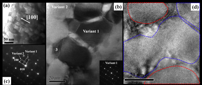
Figure 3.
(a) Plane view transmission electron microscopy image of a 110 nm GdMnO3/SrTiO3 thin film. (b) An enlarged plane view TEM image showing clear twin-like domain structure labeled with ‘variant 1' and ‘variant 2'. Small region (labeled by 3) shows ~45° rotation with respect to the two variants. The inset shows electron diffraction pattern of variant 1. (c) Electron diffraction pattern including both of variant 1 and 2. (d) High resolution TEM image of the same sample. The areas showing different variants are enclosed by blue and red lines, respectively.

