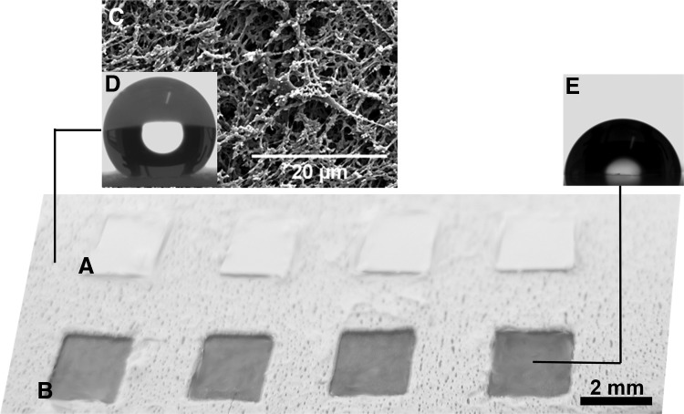
FIG. 1.
Image of a part of an array of patterns on the chip with (A) protective stickers and (B) after removing the protective stickers, with transparent wettable spots. (C) Scanning electron microscopy image of superhydrophobic domain of the chip. (D) Representative profile of a water droplet on the superhydrophobic domain of the chip (contact angle of 156.2°±0.3°). (E) Representative profile of water droplet on the nontreated part of the chip—wettable region (contact angle of 90.5°±4.7°).

