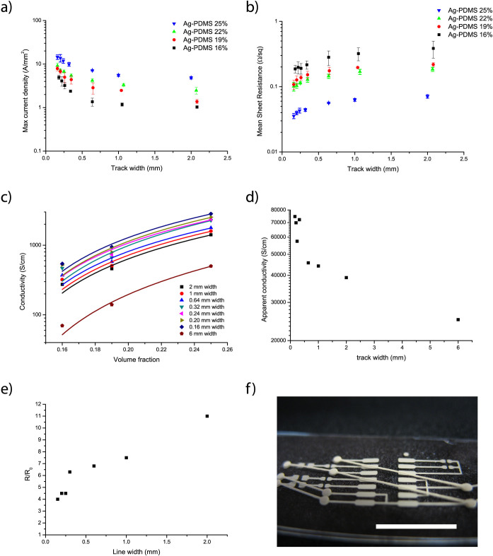
Figure 3. Stencil printing of narrow lines for the fabrication of soft PCBs.
(a) Maximum current densities and (b) sheet resistances for Ag-PDMS tracks with different widths and filler contents. (c) Mean values of measured conductivities for different tracks as a function of silver volume fraction and fitted using the percolation model with the apparent conductivity as only variable. (d) The fitted apparent conductivity as a function of track width. (e) Change in resistance after 50% strain 1 mm/s for Ag-PDMS 25vol% tracks with different widths. R is the resistance after releasing the strain and R0 is the resistance before applying the strain. (f) Picture of a double-sided PCB with vias. The large footprint in the center is for the soldering of a SOIC 14 pins packaged IC. Scale bar is 10 mm.

