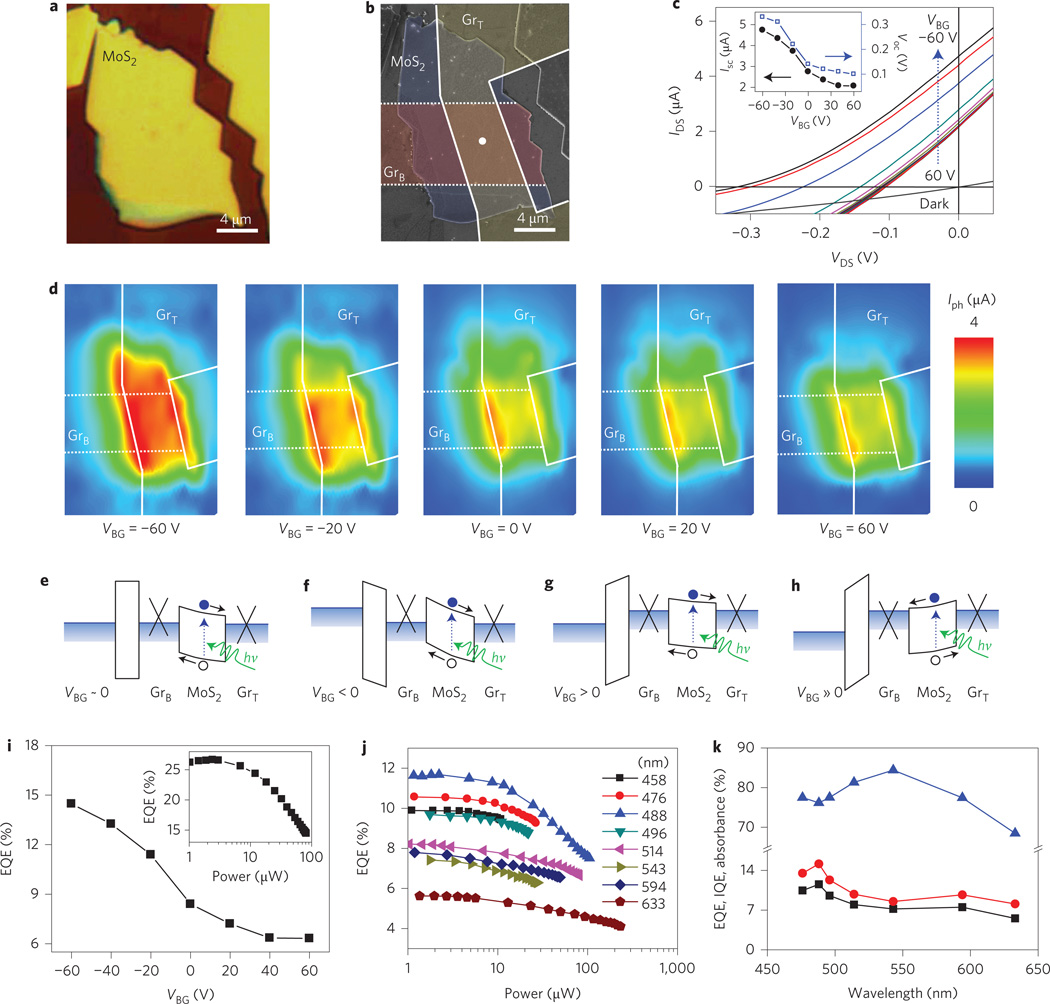
Figure 2. Field-effect modulated photocurrent generation in single-gated graphene–MoS2–graphene heterostructures.
a, Optical image of the vertical heterostructure with a multilayer MoS2 flake (~50 nm thick) sandwiched between the GrT and GrB electrodes. b, SEM image of the same device with the GrT (yellow), GrB (red) and intermediate MoS2 layer (blue) labelled with different false colours. c, I–V characteristics of the device under laser illumination (on white dot in b) at VBG varying from −60 V to +60 V in steps of 20 V. Inset: variation of Isc and Voc with VBG. d, Scanning photocurrent images taken at gate biases between −60 V and +60 V under a 514 nm laser (excitation power, 80 µW; spot size, 1 µm). Dashed and solid lines indicate the edges of the GrB and GrT electrodes, respectively. e–h, Schematic band diagrams of the vertical heterostructure with zero (e), negative (f), positive (g) and large positive (h) bias on the silicon back gate. Blue dots, black circles and green arrows indicate electrons, holes and photons, respectively. i, EQE of the vertical heterostructure device as a function of back-gate voltage under 80 µW, 514 nm laser excitation. Inset: EQE of the device as a function of excitation laser power at VBG = −60 V. j, Excitation laser power-dependent EQE of another graphene-MoS2 (16 nm)-graphene device under various excitation wavelengths at VBG = −60 V. k, Wavelength-dependent EQE (black line with squares), absorbance (red line with circles) and IQE (blue line with triangles) of the device at VBG = −60 V under a focused laser power of 5 µW.

