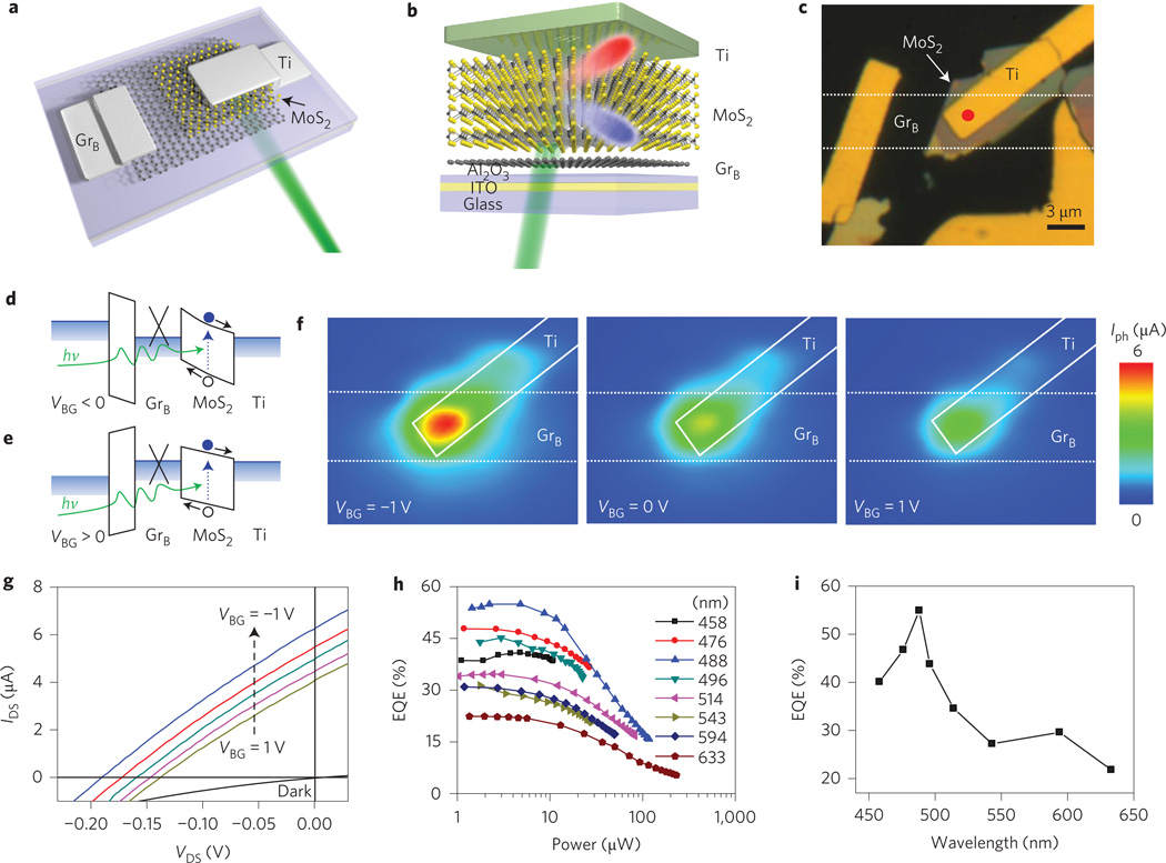
Figure 4. Field-effect modulated photocurrent generation in a single-gated graphene–MoS2–metal heterostructure.
a, Schematic three-dimensional illustration of the device layout. b, Schematic illustration of the side view of the device, with a multilayer MoS2 flake sandwiched between a GrB electrode and a top metal electrode (Ti). The device was fabricated on transparent ITO on a glass substrate (as the back gate) with 30-nm-thick Al2O3 as the gate dielectric to allow illumination to transmit through the back side of the substrate to reach the graphene–MoS2 contact. c, Optical image of a graphene–MoS2–metal heterostructure device. d,e, Schematic band diagrams of the graphene–MoS2–metal heterostructure at negative and positive back-gate voltages, respectively. f, Scanning photocurrent images taken at VBG = −1, 0 and +1 V (80µW, 514 nm excitation, with a spot size of 1 µm). Dashed and solid lines indicate the edges of the GrB and top metal electrodes, respectively. g, I–V characteristics of the device under laser illumination (on red dot in c) with VBG varying from −1 V to 1 V in steps of 0.5 V. The I–V curve obtained in the dark at VBG = −1 V passes through the origin, indicating that gate leakage is negligible. h, Excitation laser power-dependent EQE under various excitation wavelengths at VBG = −1 V. i, Wavelength-dependent EQE at a laser power of 5 µW.

