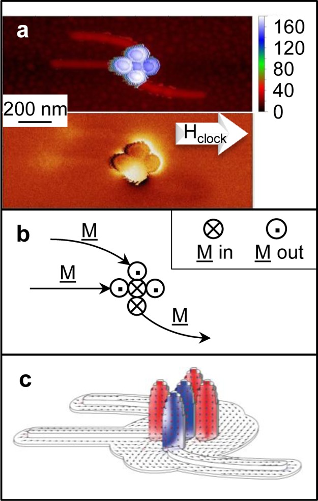
Figure 6.

3D-NML majority gate prototype of merged IP and OP nanostructures. (a) MFM investigation of the 3D array based on merged IP-NWs and OP-NPs. On one end of three inputs IP-NWs, an OP-NP has been deposited. The magnetic configuration of these three OP nanostructures is governed by the magnetization of the IP-NWs. The three input NPs are magnetically coupled to a central NP which, in turn, is magnetically coupled to the output NP. The magnetic resolution in the MFM phase shift image is limited by the relatively high lift height (∼80 nm), chosen to minimize the topography-induced artifacts. (b) The direction of the magnetization vectors in the array. (c) OOMMF simulation after Hclock removal, illustrating the orientation of the magnetization of the NPs in the 3D-NML majority gate prototype. This configuration was independent of the MS of the halo when varied between 0 and 1700 kA/m.
