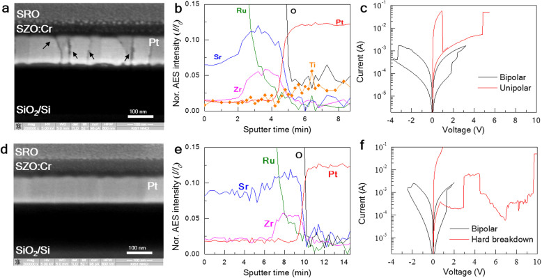
Figure 6. Structural analyses of C1 and C2 devices.
(a) SEM image of the C1 device. Traces of out-diffused Ti are observed as a linear form. (b) AES depth profile for the C1 device. Ti is detected at the SZO:Cr/Pt interface. (c) Resistive switching I–V curves for the C1 device showing RS transformation at ~5 V. (d) SEM image of the C2 device. Any trace of out-diffusion is not founded. (e) AES depth profile for the C2 device. Ti is not detected. (f) I–V curves for the C2 device. Hard dielectric breakdown occurred instead of an RS transformation.

