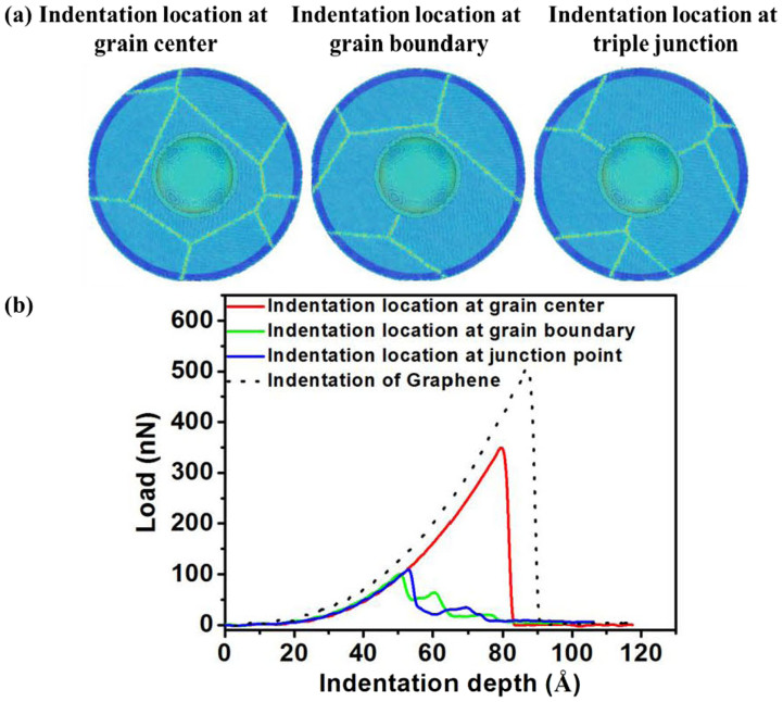
Figure 1. Failure measurements of the polycrystalline graphene indented at three different locations.
(a) The top views of indentation location at the grain center (left panel), GB (middle panel), and GB triple junction (right panel). Atoms are colored according to their von Mises stress. (b) The normal load vs. indentation depth (d) curves for three different indentation locations. The single-crystal graphene indentation result is plotted for comparison. Significant scattering in the failure load is observed for indentation on different locations.

