Figure 1.
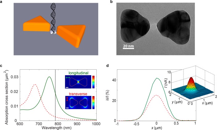
Plasmonic nanopore concept and basic characteristics. (a) Schematic illustration of a DNA molecule translocating through a plasmonic nanopore that consists of a gold bowtie antenna with a 10 nm nanopore at the gap center (not to scale). (b) TEM top-view image of a plasmonic nanopore device. (c) Simulated absorption cross sections of the plasmonic nanopore in longitudinal (green full line) and transverse (red dashed line) excitation. The black dotted line indicates the laser wavelength of 785 nm that was used in our experiments. The insets show color plots of the simulated electrical field intensity enhancement at 785 nm in the plane of the antenna and through the middle of the gold triangles (color maps from 0 to 1200 and 0 to 65 for longitudinal and transverse mode, respectively). Scale bars are 20 nm. (d) Change in current, δI, relative to the baseline current, I, for line scans of the pore through the laser focus for longitudinal (green full line) and transverse (red dashed line) mode at 0.5 mW. The inset shows a 2D scan of the variation in current along the focal plane (longitudinal mode, 100 mV bias voltage).

