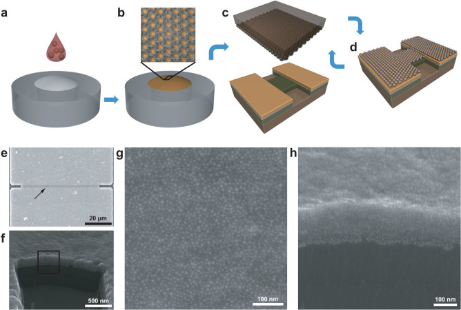
Figure 1. Schematic diagram of fabrication of two-dimensional to three-dimensional patterned close-packed nanoparticle arrays and SEM characterization of one measured device.
(a), Several drops of chloroformic solution containing octanethiol-capped gold nanoparticles were cast onto a slightly convex deionized water surface in a Teflon container. (b), With the evaporation of the solvent, nanoparticles self-assembled into an ordered compact 2D monolayer at the air/water interface, as shown in the top inset. (c), A flat PDMS stamp was used to transfer the nanoparticle sheet from the air/water interface onto the substrate surface with designed electrodes prepared using lithographic techniques. (d), Schematic of the device with one nanoparticle superlattice. By simply repeating the same transferring process, devices with a continuous change of the number of monolayers were obtained. (e), SEM image of a typical device used for the electrical measurements, which contains 15 identical nanoparticle monolayers. Magnified SEM image of the area framed by the rectangle in (e) is shown in (g). (f), Titled SEM image of the device shown in (e). Magnified SEM image of the area framed by the rectangle in (f) is shown in (h).

