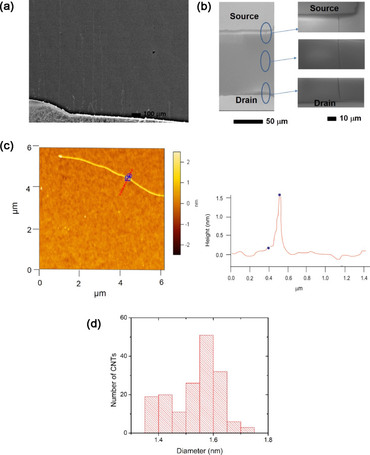
Figure 1.
FE-SEM image of (a) CVD grown SWCNTs and (b) a SWCNT FET with an enlarged view of the SWCNT near the source, central and drain regions. (c) AFM image of a single SWCNT and its height profile indicating the SWCNT diameter is ≈1.51 nm. (d) Histogram plot showing the diameter distribution of the SWCNTs. The average diameter of the SWCNTs was ≈1.53 nm.

