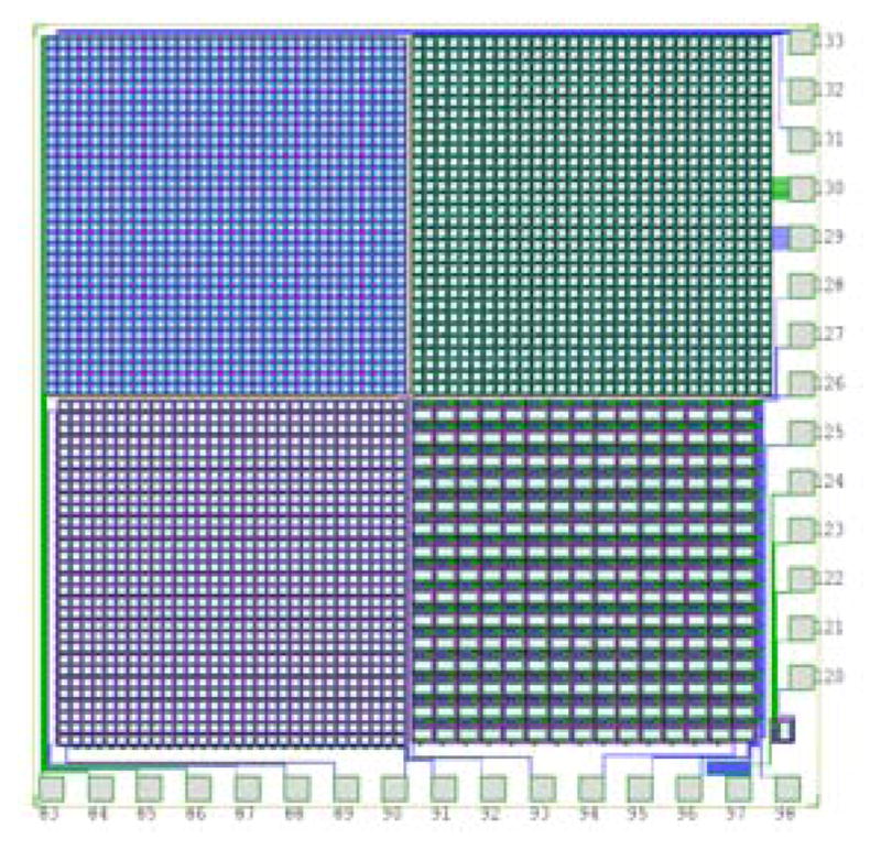
Figure 6.

Layout of the PS-SSPM chip containing four different PS-SSPM devices, designated at the AE218 chip. Each device employs a different charge division design. The “APD analog” design is the top left device, and the “row-column” design is the bottom left device.
