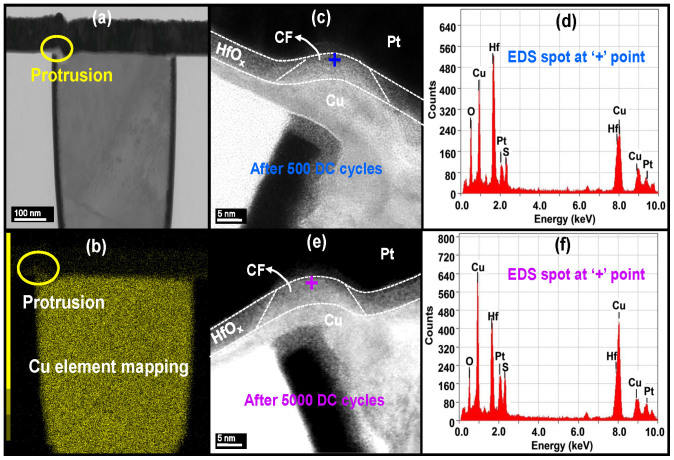
Figure 3. TEM analysis of the filament regions for the samples with different switching cycles.
(a) TEM image of the cross-section of the cycled device. A small depression can be seen at the left corner of the copper plug, resulting in a protrusion-like shape therein. (b) The copper element mapping of (a). (c) The magnification of the filament region after 500 DC cycles. The filament was located on the corner of the copper plug due to the enhancement of the local electric field. (d) EDS analysis of the spot of the filament region after 500 DC cycles. (e) The magnification of the filament region after 5000 DC cycles. This device failed at the LRS. Slight increase of the filament size was found. (f) The EDS analysis of the spots of the filament regions after 5000 DC cycles. The Cu signals after 5000 cycles were greatly enhanced from the Cu signals after 500 cycles, indicating that Cu accumulated in the filament region during cycling.

