Figure 6.

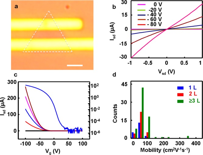
Electronic properties of WSe2 atomic layers. (a) Optical microscope image of a monolayer WSe2 transistor; scale bar is 2 μm. (b) Isd–Vsd output characteristics of the WSe2 transistor shown in panel a. (c) Isd–Vg transfer characteristics of the device shown in (a) at Vsd = 0, 1, 2, 3, and 4 V. (d) Summary of the mobility values obtained in WSe2 field effect transistors with different number of atomic layers, demonstrating a mobility range of 10–350 cm2 V–1 s–1 and maximum on/off ratio over 108.
