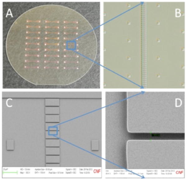
Figure 2. SCAN devices for increased throughput.
A, Optical micrograph of a 4-inch diameter fused silica wafer containing an array of 27 fluidic devices, each containing 96 parallel channels. B, Differential interference contrast optical micrograph of tens of the parallel fluidic channels in the center of a device. The square structures on each side of the central array are support pillars to prevent collapse when bonding to a cover wafer. C, Scanning electron micrograph showing approximately 8 parallel channels etched between microfluidic reservoirs on a single device. The channels are 20 microns in length (horizontal) and 500 nm deep. D, SEM close-up of an individual fluidic channel that is 750 nm in width. Devices with this parallel architecture can enable analyses like those previously reported [98, 99] with higher throughput, however, fluorescence detection will require replacing APDs with other detectors such as CMOS arrays, which will somewhat compromise sensitivity and hence throughput.

