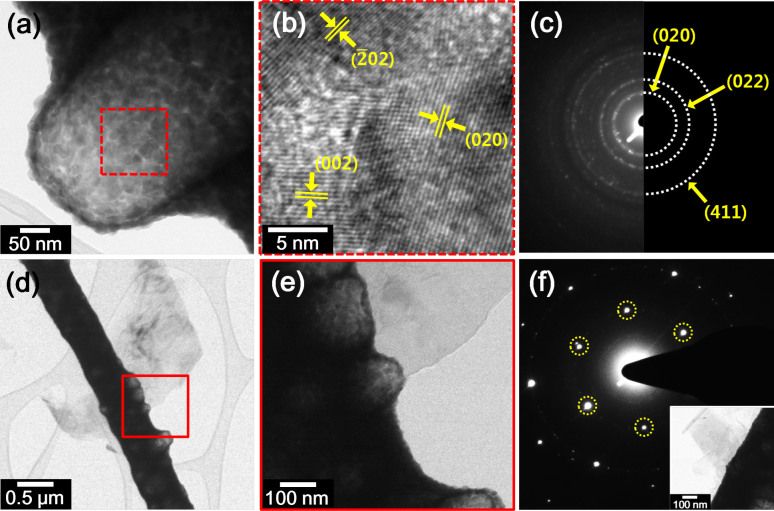
Figure 4.
(a) A TEM image of an extruded pore on the surface of a WO3 NF, (b) a magnified high-resolution TEM image of a crystallized WO3 NF (red dotted box in (a)), (c) selected area electron diffraction (SAED) pattern of WO3 NFs, (d) TEM image of a PS (500)-WO3 NF functionalized with a 0.1 wt% NOGR flake, (e) magnified TEM image of (d), and (f) SAED pattern of a PS (500)-WO3 NF functionalized with 0.1 wt% NOGR flakes with a TEM image of an electron beam illuminating the spot shown in the inset.

