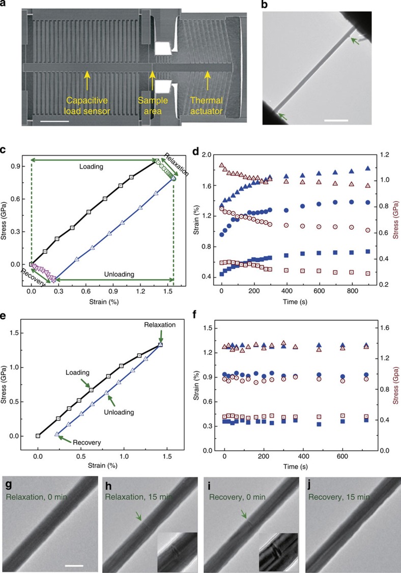
Figure 2. In situ measurements of stress and strain evolutions in Ag NWs.
(a) The MEMS stage used for in situ SEM and TEM tensile testing of Ag NWs. Scale bar, 200 nm. (b) Low-magnification TEM image of a NW bridged between the actuator and the load sensor, with two marks (arrowed) for displacement measurement. Scale bar, 500 nm. (c,e) Stress–strain curves for a penta-twinned Ag NW (120 nm in diameter) and a single-crystalline Ag NW (99 nm in diameter). Note that in both cases the relaxation and recovery steps took 15 min each. (d,f) Relaxation curves for a penta-twinned Ag NW (104 nm in diameter) and a single-crystalline Ag NW (71 nm in diameter). Note: solid and open symbols correspond to the strain–time and stress–time relationships, respectively. Square, circle and triangle symbols correspond to first, second and third stress levels, respectively. (g–j) A series of TEM images extracted from Supplementary Movies 2 and 3 showing dislocation nucleation and annihilation in a penta-twinned Ag NW (85 nm in diameter). The arrows in f,g point to the dislocation networks with high-magnification images shown in the insets. Scale bar, 150 nm.

