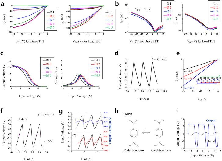
Figure 3.
(a and b) Output and transfer characteristics of the printed cnTFTs for 5 drive and 5 load TFTs respectively in the printed ring oscillator. (c) Electrical characteristics of inverters and (d) output characteristic of the ring oscillator. (e) Total output characteristics of the printed buffer unit consisting of 6 cnTFTs and a resistor (measured based on contacting gate and drain-source electrodes as shown in the inset circuit). (f) Modified triangular wave following the buffer unit. (g) Generated signals before scanning (black) and after scanning the electrochemical cells without (1, blue) and with TMPD (2, red) in a drop of solution. (h) TMPD structure for oxidation and reduction reaction. (i) The input and amplified output signals after passing through three amplifying inverters.

