Abstract
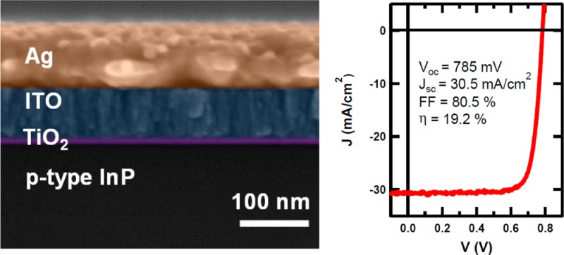
We demonstrate an InP heterojunction solar cell employing an ultrathin layer (∼10 nm) of amorphous TiO2 deposited at 120 °C by atomic layer deposition as the transparent electron-selective contact. The TiO2 film selectively extracts minority electrons from the conduction band of p-type InP while blocking the majority holes due to the large valence band offset, enabling a high maximum open-circuit voltage of 785 mV. A hydrogen plasma treatment of the InP surface drastically improves the long-wavelength response of the device, resulting in a high short-circuit current density of 30.5 mA/cm2 and a high power conversion efficiency of 19.2%.
Keywords: InP photovoltaics, titanium dioxide, heterojunctions, selective contact
Selective contacts that transmit photogenerated minority carriers and block majority carriers are key to high-performance solar cells.1 Traditionally inorganic semiconductors use doping to achieve carrier selectivity at the contacts. For organic solar cells, in contrast, transition metal oxides have proven to be efficient selective contacts.2−8 In particular TiO2 is applied widely as an electron contact in dye-sensitized solar cells,9,10 polymer solar cells,11,12 and high-performance organometallic perovskite solar cells,13−16 while substoichiometric MoOx (x < 3) has emerged as an excellent hole contact.4 Recently we demonstrated that MoOx can also serve as an efficient hole contact for n-type silicon solar cells, enabling a high open-circuit voltage of 711 mV and an efficiency of 18.8%.17,18 Analogously, TiO2 has been used as an electron-selective contact to p-type silicon.19
In this work, we show that transition metal oxides can also be applied as selective contacts for III–V solar cells. We focus in particular on InP, whose band gap of 1.35 eV lies close to the optimum for solar energy conversion.20 The most efficient InP solar cells use a homojunction configuration fabricated by metal–organic vapor deposition (MOCVD), reaching efficiencies of up to 22.1%.21 Alternatively, a shallow buried homojunction can be formed in InP by sputtering indium tin oxide (ITO) on the front surface. This approach yields efficiencies of up to 18.9%.22 In another approach, a CdS window layer is used with InP to form a heterojunction solar cell with an efficiency of 17.4%.23,24 Here, by employing a TiO2 electron contact deposited by atomic layer deposition (ALD) at a low temperature of 120 °C, we demonstrate a TiO2/InP heterojunction solar cell with a high open-circuit voltage of 785 mV and an excellent efficiency of 19.2%.
The process flow for fabricating TiO2/InP solar cells is shown in Figure 1a. Zn-doped p-type (100)-oriented InP wafers with a thickness of 350 μm and a carrier density of 2 × 1017 cm–3 are etched in HCl (6%) for 30 s to remove the native oxide. Twenty nanometers of Zn followed by 100 nm of Au are then sputtered onto the back side of the InP wafers, followed by annealing in forming gas (5% H2, 95% N2) at 420 °C for 40 min to form an ohmic back contact. TiO2 is subsequently deposited onto the front side of the InP wafers by ALD using titanium isopropoxide (Ti[OCH(CH3)2]4) and H2O as precursors. Finally, a transparent conductive oxide (ITO = In2O3:SnO = 90%:10%) electrode is sputtered on top of the TiO2 layer at room temperature in Ar ambient at a pressure of 6–7 mTorr. For all devices, the thickness of the ITO layer was adjusted according to the thickness of the TiO2 layer to maintain a total oxide thickness of ∼70 nm, such that the reflectance minimum falls in the spectral range where the solar spectrum is strongest (around a wavelength of 600 nm) in order to maximize light in-coupling into the InP absorber.17 The optimum TiO2 thickness (10 nm) maximizes the open-circuit voltage (see discussion below) and minimizes resistive losses. Photolithography followed by electron beam evaporation and lift-off were then used to define a Ag finger grid with finger width and pitch of 11 and 490 μm, respectively, to reduce series resistance. The final patterned cells have an aperture area of 5 × 5 mm2 defined by the outer Ag frame (Figure 1b). Figure 1c shows a false-colored cross section scanning electron microscopy (SEM) image of the final TiO2/p-InP heterojunction solar cell.
Figure 1.
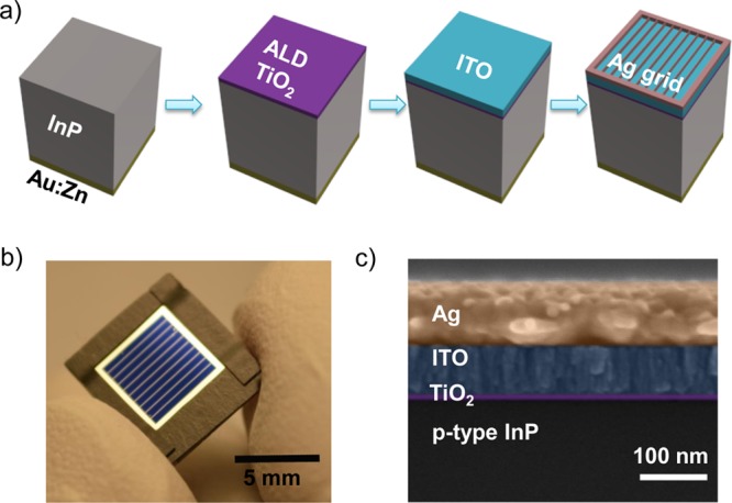
(a) Process schematics of the TiO2/InP heterojunction solar cell fabrication, depicting Au:Zn back-contact formation, ALD of TiO2 electron-selective contact, ITO sputtering, and Ag finger grid evaporation. (b) Photograph of a fully fabricated cell. The area of the cell is defined by the outer Ag frame. A black plastic tape is applied on the edges of the chip (around the outer Ag frame) to ensure no collection is obtained from outside the marked cell area. (c) False-colored, cross-sectional SEM image of a fabricated cell.
The current density–voltage (J–V) characteristics of a TiO2/InP heterojunction solar cell measured under simulated 1-sun illumination (1000 W/m2, global air mass 1.5 spectrum, 25 °C, Solar Light 16S 300W) are shown in Figure 2a. A sharp probe tip was placed on the outer Ag frame to contact the front side of the cell. Comparative tests with a four-point probe configuration gave identical results to the two-point probe configuration used here, as the Ag frame provides a contact point with negligible contact resistance to the probe tip(s). The simulated solar radiance received by the cells was calibrated to a NIST traceable silicon photodiode with similar aperture area as the InP cells and known external quantum efficiency and further cross-checked via an ISO-classified pyranometer (Solar Light PMA 2144). The error in our cell efficiency measurement is estimated to be at least 1%. A more detailed error calculation including spectral mismatch beyond class “A” would require a full spectral analysis of our solar simulator. Also shown in Figure 2a is a reference device with no TiO2 blocking layer, reaching an open-circuit voltage (Voc) of 545 mV and an efficiency of 9.9%. Insertion of the TiO2 layer leads to a dramatic increase of the Voc to 785 mV. The short-circuit current density (Jsc) also slightly improves from 24.6 mA/cm2 to 25.8 mA/cm2, resulting in an improved conversion efficiency of 15.4%. The higher Jsc is not due to a change in cell reflectance, but is attributed to improved carrier collection due to reduced recombination at the InP front interface (see Figure S1 for details). Cell performance parameters are summarized in Table 1.
Figure 2.
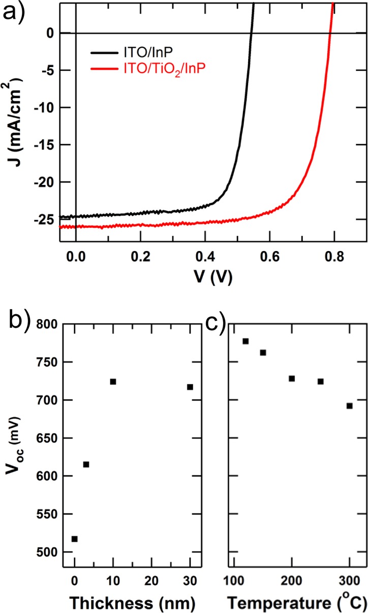
(a) Representative J–V characteristics for InP solar cells, with and without TiO2 electron-selective contact under 1-sun illumination. (b) Dependence of Voc on TiO2 thickness (at a fixed deposition temperature of 250 °C) and TiO2 deposition temperature (at a fixed thickness of 10 nm).
Table 1. Summary of InP Solar Cell Performance Parameters.
| device | Voc [mV] | Jsc [mA/cm2] | FF [%] | eff [%] |
|---|---|---|---|---|
| ITO/InP | 545 | 24.6 | 73.6 | 9.9 |
| ITO/TiO2/InP | 785 | 25.8 | 72.8 | 15.4 |
| ITO/TiO2/InP with H2 plasma | 785 | 30.5 | 80.1 | 19.2 |
To optimize device performance, we investigate the dependence of Voc on the TiO2 thickness and deposition temperature (see Figure 2b and c, respectively). For each condition, at least three devices were fabricated and measured, and the average Voc values are reported here. When deposited at a fixed temperature of 250 °C, the Voc increases rapidly with increasing TiO2 thickness and reaches a saturation value of 740 mV for a thickness of 10 nm, beyond which the Voc does not change significantly (Figure 2b). Lowering the deposition temperature to 120 °C at a fixed thickness of 10 nm increases the Voc further to 780 mV (Figure 2c).
In order to better understand the Voc improvement due to the insertion of the TiO2 layer, we characterized the structural and electronic properties of ALD TiO2. Raman spectroscopy (Figure S2a) indicates that TiO2 deposited at 120 °C, for which we observed the highest Voc, is in an amorphous phase in agreement with literature.25 Atomic force microscopy (Figure S2b and c) reveals a smooth, relatively featureless, film morphology consistent with an amorphous film structure (root-mean-square (rms) roughness 0.3 nm). In contrast, TiO2 films deposited at 250 °C exhibit a weak Raman signal at 140 cm–1 corresponding to a nanocrystalline anastase phase and a rougher surface morphology consistent with the formation of small crystallites (rms roughness 1.2 nm).
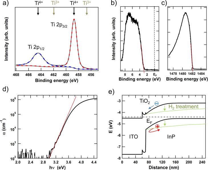
Figure 3a presents the X-ray photoelectron spectrum (XPS) of the Ti 2p core level of the ALD TiO2 layer deposited at 120 °C measured with monochromated Al Kα photons with an energy of 1486.7 eV. The core level is spin split into the 2p3/2 and 2p1/2 doublet centered at 458.7 and 464.4 eV, respectively, corresponding to the Ti4+ valence state of the Ti atoms.26 No appreciable signal from the Ti3+ components, typically located at 462.0 and 456.8 eV (see arrows in Figure 3a), is detected. Also a satisfactory fit obtained by adding only two Voigtian components for the Ti4+ doublet on top of a Shirley background indicates that our films are close to stoichiometric TiO2 (see SI S5 for technical details). A fit including four Voigtian components for the Ti4+ and Ti3+ doublets results in the Ti3+ peaks vanishing during convergence, indicating no detectable evidence for oxygen vacancies with Ti3+ configuration.
Figure 3.
X-ray photoelectron spectra for (a) Ti 2p core level (vertical arrows indicate the energy positions of the Ti4+ and Ti3+ valence states), (b) the valence band region with the Fermi level (EF) at zero binding energy, and (c) the secondary electron cutoff of 10 nm TiO2 on a p-InP wafer, deposited at 120 °C. (d) Absorption coefficient as a function of photon energy for an ALD TiO2 film on glass. (e) Schematic band diagram of the TiO2/InP heterojunction solar cell simulated by PC1D.36 The horizontal axis represents the distance away from the top surface, and the vertical axis shows the energy with respect to the vacuum level. The extended space charge region in InP after the H2 plasma treatment is indicated by light green lines. A work function of 4.3 eV and electron affinity of 4.4 eV were assumed for ITO.37
Figure 3b shows the valence band spectrum of the TiO2 film, which is dominated by O 2p states. Consistent with the conclusion from the Ti 2p core level, we do not observe evidence for an oxygen-vacancy-derived defect band in the band gap of TiO2 (compare for example to MoOx, where such a defect band is clearly observed17). A linear extrapolation (red line) of the valence band edge fixes the valence band maximum at 2.9 eV below the Fermi level located at zero binding energy (dashed black line). Figure 2c shows the secondary electron cutoff of the photoelectron spectrum (the spectra are corrected for an externally applied bias of −9 V on the sample, which accelerates photoelectrons away from the sample into the detector), from which we extract the workfunction by subtracting the cutoff energy of 1482.2 eV determined again by linear extrapolation (red line) from the photon energy of 1486.7 eV. Thus, the work function of TiO2 is determined to be 4.5 eV.
To determine the optical band gap of our TiO2, we measured the absorption coefficient of a TiO2 film deposited on a glass substrate (Figure 3d). Typical for an amorphous material, we observe a tail in the absorption spectrum that rises exponentially toward higher energy. The Tauc band gap determined to be the energy where the absorption coefficient starts to deviate from the exponential (red line in log scale) is 3.4 eV, which is slightly higher than the value of 3.2 eV reported for crystalline anastase TiO2.27
From the position of the Fermi level with respect to the vacuum level given by the workfunction and the valence band maximum determined with respect to the Fermi level, we conclude that the valence band maximum of TiO2 is located at 7.4 eV below the vacuum level. Together with the information on the optical band gap, the conduction band minimum consequently falls at 4.0 eV below the vacuum level.
A similar analysis for the InP surface (Figure S3) places the valence band of InP at 5.4 eV below the vacuum level. With a band gap of 1.35 eV, the conduction band maximum falls to 4.05 eV. These values are roughly consistent with values determined by the Mott–Schottky technique, which confirms that the conduction band of TiO2 (4.3 eV) is energetically well matched to that of InP (4.2 eV) although slightly further away from vacuum.28 More detailed investigations are necessary to compare and unify band positions extracted from different experimental techniques.29
The Fermi level of InP as determined by XPS is located 0.6 eV above the valence band maximum (see Figure S3a). It is important to note that due to the extreme surface sensitivity of XPS, this value represents the surface Fermi level and may be heavily affected by surface defects, surface oxidation, or charge transfer from surface adsorbates (Figure S3c). The position of the Fermi level in the InP bulk can be calculated from the hole concentration (2 × 1017 cm–3) and is located 0.1 eV above the valence band maximum. Consequently the bare InP surface already exhibits some band bending at the surface. In fact, it is well known that intentional surface defect formation via ion bombardment of the InP surface can lead to type conversion resulting in buried homojunctions.30 However, here the bare InP surface is still slightly p-type, as the position of the intrinsic Fermi level in InP lies 700 mV above the valence maximum (slightly above midgap due to the different effective masses between electrons and holes).
On the basis of these results, we draw the band diagram for the TiO2/p-InP heterostructure shown in Figure 3e. At equilibrium, the Fermi level of TiO2 aligns with the Fermi level of InP, inducing an inversion region in p-type InP close to the TiO2/InP interface. Minority electrons generated by the absorbed photons in InP can easily diffuse toward the front contact and do not experience a barrier at the TiO2 interface. Majority holes in contrast are prohibited from flowing into the front contact due to the combined effect of the band bending in the space charge region and the very large band offset (∼2 eV) between the valence band of InP and the valence band of TiO2. Therefore, TiO2 acts as an efficient electron-selective contact for InP.
While the Voc obtained with TiO2 compares well with the best values reported for ITO/InP buried homojunction and CdS/InP heterojunction cells (Table 2), the Jsc turns out to be much lower. External quantum efficiency (EQE) measurements shown in Figure 4a reveal that the low current can be attributed to a poor long-wavelength response of the TiO2/InP solar cell (black line). The reduction in EQE toward the infrared is only partially due to reflectance losses. As the TiO2 and ITO thicknesses were optimized to minimize reflectance in the spectral range around 600 nm, the reflectance (shown as 1-R in Figure 4a) increases continuously toward longer wavelengths. This is expected for an antireflection coating that relies on destructive interference between incoming and reflected light to cancel reflection. However, the EQE drops much faster toward the band edge of InP than the 1-R curve. Thus, the poor infrared response cannot be explained solely by reflectance losses, but must also be attributed to collection losses.
Table 2. Comparison of State-of-the-Art InP Solar Cell Performance Parameters (Measured under AM1.5, for Cell Areasc).
| device type | description | Voc [mV] | Jsc [mA/cm2] | FF [%] | eff [%] | ref |
|---|---|---|---|---|---|---|
| MOCVD | homojunction | 878 | 29.5 | 85.4 | 22.1 | (21), (30) |
| TiO2/InP | heterojunction | 785 | 30.5 | 80.1 | 19.2 | this work |
| ITO/InP | buried homojunction | 813 | 28.0 (28.2a) | 82.9 | 18.9 | (22) |
| CdS/InP | heterojunction | 750 | 32.3 (28.6b) | 72.0 | 17.4 | (24) |
After applying recalibration due to replacement of the IEC 60904-3 Ed. One (1989) standard by the IEC 60904-3 Ed. Two (2008) standard.31
Extracted from EQE using IEC 60904-3 Ed. Two (2008) standard.
The total cell area of the current InP world record cell is specified as 4.02 cm2 in ref (30). No further details are given. The ITO/InP cell in ref (22) is reported to have a mesa area of 0.108 cm2, of which 5% is shaded by the Au finger grid. The TiO2/InP cell described in this work has an area of 0.25 cm2 masked by the outer Ag frame (Figure 1b), of which 2% is shaded by the Ag finger grid. Ref (25) specifies a diameter of 1.5 mm for the CdS/InP cells, but cell area/shape and grid shading are not specified.
Figure 4.
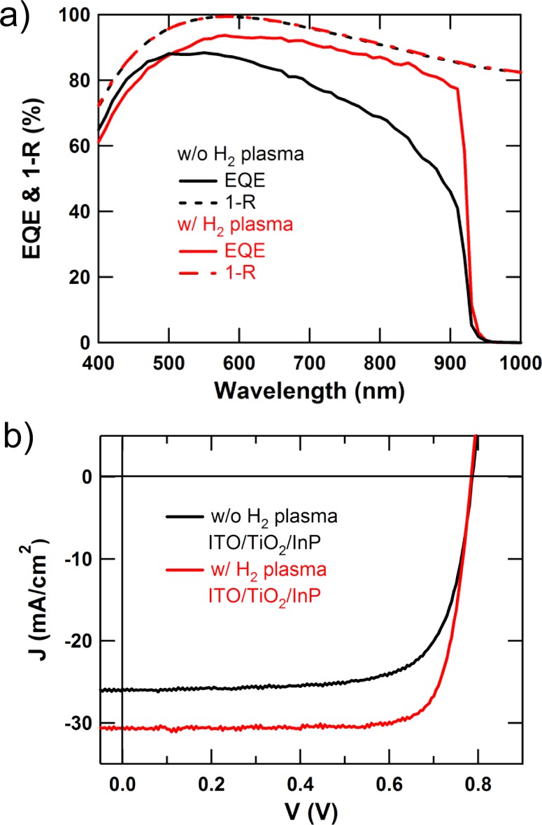
(a) EQE, 1-R, and (b) J–V characteristics measured under 1-sun for TiO2/InP solar cells, with and without H2 plasma treatment prior to ALD of TiO2.
We recently showed using electron-beam-induced current (EBIC) measurements that the effective minority carrier collection length in InP can be increased dramatically from 0.5 μm to 2.6 μm by reactive ion etching in a H2:CH4:Ar ambient, resulting in a much enhanced near-band-gap response in the EQE.32 In addition, it is well known that hydrogen effectively neutralizes shallow acceptors in InP, resulting in a decrease in effective hole concentration and an extension of the effective minority carrier collection depth (see Figure 3e).33,34 However, these buried homojunction-type cells suffered from a strongly suppressed response at short wavelengths due to the formation of a defective surface layer with strong nonradiative recombination limiting cell efficiencies to 14.4%.
In order to boost the long-wavelength response, while maintaining a strong short-wavelength response, we subjected the front side of the InP wafers to a H2 plasma (pressure of ∼85 mTorr, power density of 0.5 W/cm2, and bias voltage of −450 V) before TiO2 deposition. The H2 plasma causes the loss of phosphorus and formation of indium droplets at the InP surface, as shown in Figure S4, which are detrimental for device performance. To eliminate these indium residues, the InP surface was wet etched in piranha solution (H2SO4/H2O2 = 10:1) for 30 s and rinsed in deionized water, which leaves a flat specular surface similar to InP before H2 plasma treatment.
As shown in Figure 4a, the H2 plasma treatment leads to a dramatic increase of the EQE (shown in red) over a wide spectral range, reaching from 500 nm all the way up to the band gap at 920 nm. As expected, the reflectance of the H2 plasma treated cell remains identical to the cell without H2 plasma treatment. The EQE now follows the 1-R curves closely, indicating much reduced collection losses. Remarkably the short-wavelength response remains almost unaffected and is maintained above 60% at 400 nm. Figure 4b compares the 1-sun J–V curves for cells with and without H2 plasma treatment. The Voc remains unchanged, reaching 785 mV for the best cell. The enhanced EQE due to the H2 plasma treatment accounts for a massive gain in Jsc of 4.7 mA/cm2, resulting in an excellent photocurrent of 30.5 mA/cm2. This current could be further improved by applying an additional MgF2 antireflection coating. Combined with a fill factor of 80.1%, a high efficiency of 19.2% is reached.
As for the role of the H2 plasma treatment versus TiO2, the former enhances band bending, which helps in collecting minority carriers generated by long-wavelength photons and consequently improves the red response. On the other hand, TiO2 provides a large barrier for majority holes (associated with the large valence band offset with respect to InP) but allows minority electrons to pass through (due to the small conduction band offset with respect to InP). This reduces the dark current and therefore improves Voc. From experimental data, band bending induced by H2 plasma treatment alone is not sufficient to reach high Voc. Table 2 compares the performance parameters of our TiO2/InP heterojunction solar cell with the values reported in the literature for alternative device configurations. Remarkably, our heterojunction solar cell reaches the highest efficiency after the world record InP homojunction solar cell fabricated by expensive MOCVD. In particular, our cell fabrication process is compatible with InP thin films grown directly on cheap metal foils using our recently developed thin film vapor liquid solid growth technique,35 which circumvents the main cost drivers for III–V photovoltaics: the epitaxial wafer substrate, low precursor utilization yield, and long growth times associated with MOCVD. Our cell configuration therefore provides a promising route toward low-cost large-area III–V photovoltaics with high efficiency.
In conclusion, we have demonstrated a simple TiO2/InP heterojunction solar cell achieving an efficiency of 19.2% using an electron-selective TiO2 contact prepared by ALD. A H2 plasma treatment substantially improves the spectral response of the cell. Importantly our process is fully compatible with InP thin films, rendering InP interesting not only for space applications but also for terrestrial deployment.
Acknowledgments
This work was funded by the Bay Area Photovoltaics Consortium (BAPVC). TiO2 deposition and characterization was funded by the Director, Office of Science, Office of Basic Energy Sciences, Material Sciences and Engineering Division of the U.S. Department of Energy, under Contract No. DE-AC02-05CH11231. X.Y. acknowledges a scholarship from the China Scholarship Council (CSC). C.B. acknowledges support from the Zeno Karl Schindler Foundation.
Supporting Information Available
Additional materials and device characterization data. This material is available free of charge via the Internet at http://pubs.acs.org.
The authors declare no competing financial interest.
Funding Statement
National Institutes of Health, United States
Supplementary Material
References
- Würfel P.Physics of Solar Cells: From Principles to New Concepts; Wiley: Weinheim, Germany, 2005. [Google Scholar]
- Shrotriya V.; Li G.; Yao Y.; Chu C.-W.; Yang Y. Transition metal oxides as the buffer layer for polymer photovoltaic cells. Appl. Phys. Lett. 2006, 88, 073508. [Google Scholar]
- Xie F.; Choy W. C. H.; Wang C.; Li X.; Zhang S.; Hou J. Low-temperature solution-processed hydrogen molybdenum and vanadium bronzes for an efficient hole-transport layer in organic electronics. Adv. Mater. 2013, 25, 2051–2055. [DOI] [PubMed] [Google Scholar]
- Sun Y.; Takacs C. J.; Cowan S. R.; Seo J. H.; Gong X.; Roy A.; Heeger A. J. Efficient, air-stable bulk heterojunction polymer solar cells using MoOx as the anode interfacial layer. Adv. Mater. 2011, 23, 2226–2230. [DOI] [PubMed] [Google Scholar]
- Irwin M. D.; Buchholz D. B.; Hains A. W.; Chang R. P. H.; Marks T. J. p-Type semiconducting nickel oxide as an efficiency-enhancing anode interfacial layer in polymer bulk-heterojunction solar cells. Proc. Natl. Acad. Sci. U.S.A. 2008, 105, 2783–2787. [Google Scholar]
- Chen C.-P.; Chen Y.-D.; Chuang S.-C. High-performance and highly durable inverted organic photovoltaics embedding solution-processable vanadium oxides as an interfacial hole-transporting layer. Adv. Mater. 2011, 23, 3859–3863. [DOI] [PubMed] [Google Scholar]
- Tao C.; Ruan S.; Xie G.; Kong X.; Shen L.; Meng F.; Liu C.; Zhang X.; Dong W.; Chen W. Role of tungsten oxide in inverted polymer solar cells. Appl. Phys. Lett. 2009, 94, 043311. [Google Scholar]
- Tan Z.; Li L.; Cui C.; Ding Y.; Xu Q.; Li S.; Qian D.; Li Y. Solution-processed tungsten oxide as an effective anode buffer layer for high-performance polymer solar cells. J. Phys. Chem. C 2012, 116, 18626–18632. [Google Scholar]
- O’Regan B.; Grätzel M. A low-cost, high-efficiency solar cell based on dye-sensitized colloidal TiO2 films. Nature 1991, 353, 737–740. [Google Scholar]
- Burke A.; Ito S.; Snaith H.; Bach U.; Kwiatkowski J.; Gretzel M. The function of a TiO2 compact layer in dye-sensitized solar cells incorporating “planar” organic dyes. Nano Lett. 2008, 8, 977–981. [DOI] [PubMed] [Google Scholar]
- Mor G. K.; Kim S.; Paulose M.; Varghese O. K.; Shankar K.; Basham J.; Grimes C. A. Visible to near-infrared light harvesting in TiO2 nanotube array-P3HT based heterojunction solar cells. Nono Lett. 2009, 9, 4250–4257. [DOI] [PubMed] [Google Scholar]
- You J.; Chen C.-C.; Dou L.; Murase S.; Duan H.-S.; Hawks S. A.; Xu T.; Son H. J.; Yu L.; Li G.; Yang Y. Metal oxide nanoparticles as an electron-transport layer in high-performance and stable inverted polymer solar cells. Adv. Mater. 2012, 24, 5267–5272. [DOI] [PubMed] [Google Scholar]
- Liu M.; Johnston M. B.; Snaith H. J. Efficient planar heterojunction perovskite solar cells by vapour deposition. Nature 2013, 501, 395–398. [DOI] [PubMed] [Google Scholar]
- Burschka J.; Pellet N.; Moon S.-J.; Humphry-Baker R.; Gao P.; Nazeeruddin M. K.; Gratzel M. Sequential deposition as a route to high-performance perovskite-sensitized solar cells. Nature 2013, 499, 316–319. [DOI] [PubMed] [Google Scholar]
- Juarez-Perez E. J.; Wuβler M.; Fabregat-Santiago F.; Lakus-Wollny K.; Mankel E.; Mayer T.; Jaegermann W.; Mora-Sero I. Role of the selective contacts in the performance of lead halide perovskite solar cells. J. Phys. Chem. Lett. 2014, 5, 680–685. [DOI] [PubMed] [Google Scholar]
- Lee M. M.; Teuscher J.; Miyasaka T.; Murakami T. N.; Snaith H. J. Efficient hybrid solar cells based on meso-superstructured organometal halide perovskites. Science 2013, 338, 643–647. [DOI] [PubMed] [Google Scholar]
- Battaglia C.; Yin X.; Zheng M.; Sharp I. D.; Chen T.; McDonnell S.; Azcatl A.; Carraro C.; Ma B.; Maboudian R.; Wallace R. M.; Javey A. Hole selective MoOx contact for silicon solar cells. Nano Lett. 2014, 14, 967–971. [DOI] [PubMed] [Google Scholar]
- Battaglia C.; de Nicolás S. M.; De Wolf S.; Yin X.; Zheng M.; Ballif C.; Javey A. Silicon heterojunction solar cell with passivated hole selective MoOx contact. Appl. Phys. Lett. 2014, 104, 113902. [Google Scholar]
- Avasthi S.; McClain W. E.; Man G.; Kahn A.; Schwartz J.; Sturm J. C. Hole-blocking titanium-oxide/silicon heterojunction and its application to photovoltaics. Appl. Phys. Lett. 2013, 102, 203901. [Google Scholar]
- Loferski J. J. Theoretical considerations governing the choice of the optimum semiconductor photovoltaic solar energy conversion. J. Appl. Phys. 1956, 27, 777–784. [Google Scholar]
- Keavney C. J.; Haven V. E.; Vernon S. M.; Emitter structures in MOCVD InP solar-cells. Conference Record of the Twenty First IEEE Photovoltaic Specialists Conference - 1990, Vol. 1; 1990; pp 141–144.
- Li X.; Wanlass M. W.; Gessert T. A.; Emery K. A.; Coutts T. J. High-efficiency indium tin oxide indium-phosphide solar cells. Appl. Phys. Lett. 1989, 54, 2674–2676. [Google Scholar]
- Wagner S.; Shay J. L.; Bachmann K. J.; Buehler E. p-InP/n-CdS solar cells and photovoltaic detectors. Appl. Phys. Lett. 1975, 26, 229–230. [Google Scholar]
- Saito S.; Hashimoto Y.; Ito K. Efficient ZnO/CdS/lnP heterojunction solar cell. In 1994 IEEE First World Conference on Photovoltaic Energy Conversion/Conference Record of the Twenty Fourth IEEE Photovoltaic Specialists Conference, Vol 2; 1994; pp 1867–1870.
- Aarik J.; Aidla A.; Uustare T.; Sammelselg V. Morphology and structure of TiO2 thin films grown by atomic layer deposition. J. Cryst. Growth 1995, 148, 268–275. [Google Scholar]
- Wagner C. D.; Riggs W. M.; Davis L. E.; Moulder J. F.; Muilenberg G. E.. Handbook of X-ray Photoelectron Spectroscopy; Perkin-Elmer Corporation: MN, 1979. [Google Scholar]
- Tang H.; Prasad K.; Sanjinès R.; Schmid P. E.; Lévy F. Electrical and optical properties of TiO2 anatase thin films. J. Appl. Phys. 1994, 75, 2042–2047. [Google Scholar]
- Lin Y.; Kapadia R.; Yang J.; Zheng M.; Chen K.; Hettick M.; Yin X.; Battaglia C.; Sharp I.; Ager J. W.; Javey A. p-InP photocathode with titanium oxide hole blocking layer for efficient solar hydrogen production. Submitted.
- Detert D. M.; Tom K.; Battaglia C.; Denlinger J.; Lim S. H. M.; Javey A.; Anders A.; Dubon O. D.; Yu K. M.; Walukiewicz W. Fermi level stabilization and band edge energies in CdxZn1-xO Alloys. J. Appl. Phys. 2014, 115, 233708. [Google Scholar]
- Green M.; Emery K.; Hishikawa Y.; Warta W.; Dunlop E. D. Solar cell efficiency table (version 43). Prog. Photovoltaics: Res. Appl. 2014, 22, 1–9. [Google Scholar]
- Green M.; Emery K.; Hishikawa Y.; Warta W. Solar cell efficiency tables (Version 33). Prog. Photovoltaics: Res. Appl. 2009, 17, 85–94. [Google Scholar]
- Battaglia C.; Xu J.; Zheng M.; Yin X.; Hettick M.; Chen K.; Haegel N.; Javey A. Enhanced near-bandgap response in InP nanopillar solar cells. Adv. Energy Mater. 2014, 10.1002/aenm.201400061. [DOI] [Google Scholar]
- Hayes T. R.; Dautremont-Smith W. C.; Luftman H. S.; Lee J. W. Passivation of acceptors in InP resulting from CH4/H2 reactive ion etching. Appl. Phys. Lett. 1989, 55, 56–58. [Google Scholar]
- Dautremont-Smith W. C.; Lopata J.; Pearton S. J.; Koszi L. A.; Stavola M.; Swaminathan V. Hydrogen passivation of acceptors in p-InP. J. Appl. Phys. 1989, 66, 1993–1996. [Google Scholar]
- Kapadia R.; Yu Z.; Wang H.-H. H.; Zheng M.; Battaglia C.; Hettick M.; Kiriya D.; Takei K.; Lobaccaro P.; Beeman J. W.; Ager J. W.; Maboudian R.; Chrzan D. C.; Javey A. A direct thin-film path towards low-cost large-area III-V photovoltaics. Sci. Rep. 2013, 3, 2275. [DOI] [PMC free article] [PubMed] [Google Scholar]
- Basore P. A. Numerical modelling of textured silicon solar cells using PC-1D. IEEE Trans. Electron Devices 1990, 37, 337. [Google Scholar]
- Schlaf R.; Murata H.; Kafafi Z. H. Work function measurements on indium tin oxide films. J. Electron Spectrosc. Relat. Phenom. 2001, 120, 149–154. [Google Scholar]
Associated Data
This section collects any data citations, data availability statements, or supplementary materials included in this article.


