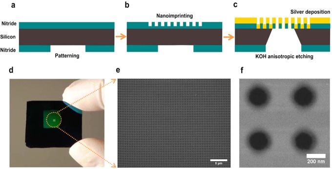
Figure 1.
Fabrication of suspended nanohole array chip. (a) A silicon chip after 200 nm low-stress nitride deposition and photolithography to expose desired regions on the backside. (b) Nanoimprinting and dry etching was performed to transfer the nanohole array pattern to the top nitride membrane. Nanoimprint resist was then washed away. (c) Anisotropic KOH etching of silicon was used to obtain the suspended nitride membrane. A final dry etch removed the remaining nitride from the bottom of the holes. Silver was then evaporated from the top to obtain suspended metallic nanohole arrays. (d) A 1 in. × 1 in. chip with a 1 cm × 1 cm nanoimprinted region in the center. The nanoimprinted region further has a 1 mm × 1 mm suspended membrane in the center (circled). (e) SEM image of the suspended membrane with nanoholes. (f) SEM shows magnified image of the individual nitride nanoholes.

