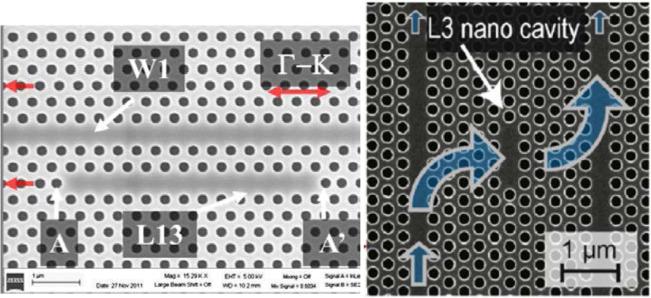
Fig. 13.
SEM images of sensor designs in which a point-like defect is placed within the vicinity of a bus W1 waveguide to allow evanescent side coupling from the waveguide to the cavity. (left) From ref. [79] with permission from Elsevier, copyright 2012. (right) From ref. [65] with permission from Elsevier, copyright 2009.

