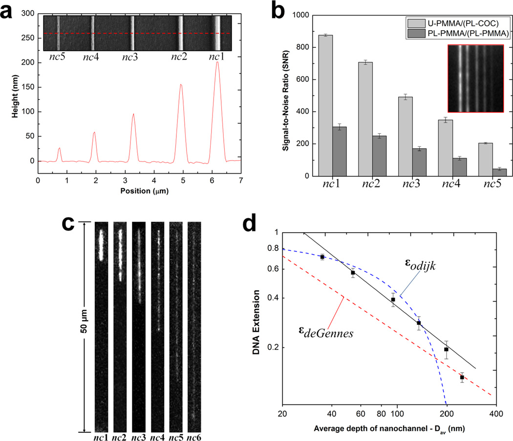
Figure 5.
(a) AFM scan and SEM image (insert) of the UV curable resin stamp possessing a positive tone of the 2-D nanochannels. Channels were imprinted into PMMA with dimensions (width × depth) of nc1 = 300 × 200 nm, nc2 = 250 × 155 nm, nc3 = 190 × 95 nm, nc4 = 150 × 60 nm and nc5 = 110 × 25 nm. (b) Bar graphs showing the signal-to-noise ratio (SNR) at 2 s exposure time for the devices with untreated PMMA substrate enclosed with a plasma treated COC cover plate, U-PMMA/(PL-COC), and plasma treated substrate enclosed with a plasma treated PMMA cover plate, PL-PMMA/(PL-PMMA) filled with a 5 mM FITC solution. The error bars represent the standard deviation in measurements from ten separate devices. Insert shows unprocessed images of the seeding test for U-PMMA/(PL-COC). (c) Unprocessed representative frames of T4 DNA molecules elongated in enclosed nanochannels for the hybrid devices. Images were acquired at 10 ms exposure time with the driving field turned-off. Note that nc6 = 35 × 35 nm. (d) Log-log plot showing the T4 DNA extension as a function of the geometric average depth of the nanochannels. The DNA extension was normalized to a total contour length (Lc) of 64 µm for the dye-labeled molecules. The red and blue dashed lines are the deGennes and Odijk predictions, respectively. The black solid line is the best power-law fit to the data points obtained from the nanochannels with an average geometric depth range of 53 nm to 200 nm.

