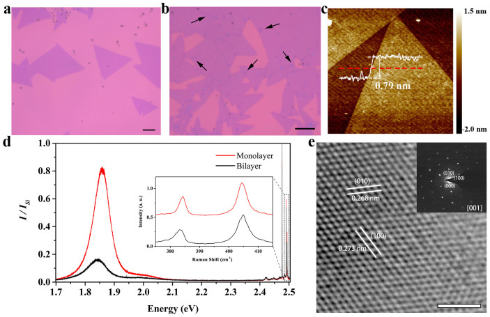
Figure 1. Synthesis and characterization of monolayer MoS2.
(a) and (b) Optical images of typical MoS2 on 280 nm SiO2/Si substrates synthesized by CVD method. The growth durations are 10 min and 20 min, respectively. In (b), some monolayer MoS2 islands overlapped with one another because of the longer growth time, as indicated with arrows. The scale bars correspond to 10 μm. (c) AFM image of two neighbored MoS2 triangular islands. The white curve shows the thickness along the red dashed line. The scale bar corresponds to 0.5 μm. (d) Room-temperature PL spectra from monolayer MoS2 (red) and bilayer MoS2 (black). Peak height is normalized to the silicon Raman peak. Raman signals also appear in the PL spectra at the higher energy, details of which are shown in the inset. (e) HRTEM image of freely suspended monolayer MoS2. The inset is the corresponding SAED pattern recorded along the [001] zone axis. The scale bar corresponds to 2 nm.

