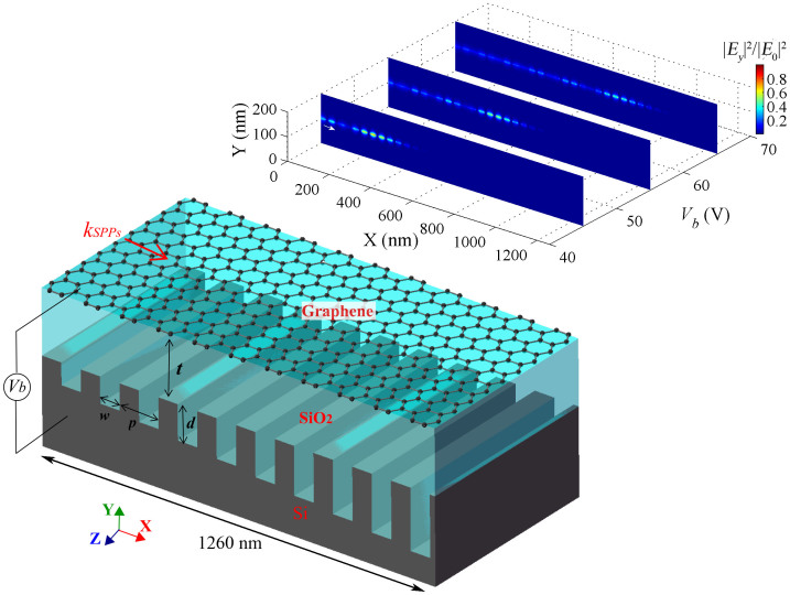
Figure 3. Schematic illustration of the graphene plasmonic graded grating structure.
The groove depth d increases gradually along the direction of light propagation. p, w and t are the grating period, the groove width and the thickness of SiO2 spacer, respectively. The inset shows cross-sectional contour plots of the field distribution |Ey|2 along the graphene at the wavelength of 9.0 μm for different gate voltages. |E0| is the maximum value of |Ey|. In the simulation, the parameters are set as t = 100 nm, p = 2w = 40 nm, T = 300 K and μ = 20000 cm2V−1s−1. d increases linearly from 100 nm to 400 nm with an increment of 10 nm.

