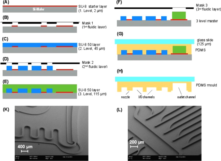
FIG. 1.
Fabrication flow of three-layer lithography and PDMS micro-molding. (A) SU8-25 photoresist deposition, thickness 2 μm, (B) 1st lithography step, (C) SU8-50 photoresist deposition, thickness 45 μm, (D) 2nd lithography step, (E) SU8-50 photoresist deposition, thickness 115 μm (F) 3rd lithography step, (G) PDMS molding, (H) releasing the PDMS replica, and (K) and (L) SEM images of patterned photoresist combination of SU8-25/50.

