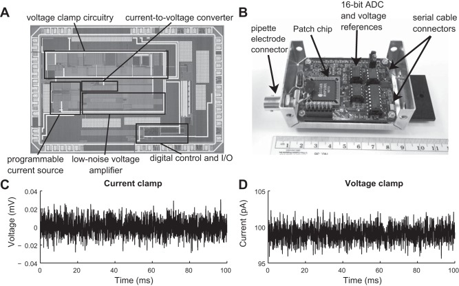
Fig. 3.
PatchChip design and benchtop characteristics. A: microphotograph of the PatchChip. Each silicon chip measures 4.7 × 3.0 mm and contains more than 20,000 transistors, resistors, and capacitors. B: circuit board containing the PatchChip [in black plastic leaded chip carrier (PLCC) package labeled “Intan”] and supporting components. The aluminum enclosure (measuring 8.5 × 5.7 × 2.9 cm) shields the sensitive electronics from interference. This circuit board contains the functionality of the head stage as well as the rack-mounted amplifier and analog-to-digital converter (ADC) in traditional patch-clamp amplifier systems. All current and voltage measurements are digitized on this circuit board and passed to a USB interface board over digital serial cables. C: measured voltage noise floor of PatchChip in current-clamp (injected I = 0) mode. Noise over the 10-kHz bandwidth was 8.2 μV root mean square (rms). D: measured current noise floor of PatchChip in voltage-clamp mode measuring 100 pA in current. Noise over the 5-kHz bandwidth was 1.1 pA rms.

