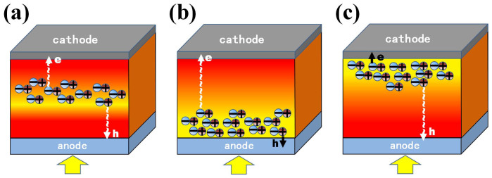
Figure 1. The conceptual diagram of plasmonic-electrical effect.
Light absorption is spatially redistributed at the active layer for manipulating transport paths of photocarriers (minus and plus notations denote electrons and holes, respectively). A desired light absorption distribution is realized by spatially tuning the position of metallic NPs with strongly localized plasmonic effects. Light absorption of active materials is optimized by spectrally tuning the shape-dependent plasmonic resonance. The arrows e and h are the transport paths of electrons and holes. Generated electron-hole pairs (excitons) are concentrated (a) at the middle of the active layer, (b) near the anode, and (c) near the cathode, respectively.

