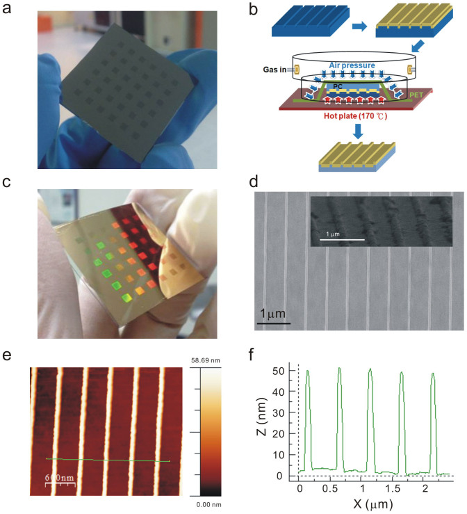
Figure 6. Fabrication of capped gold nanoslits using a thermal annealing-assisted template stripping method.
(a) The optical image of the fabricated silicon template. There are 6 × 6 groove arrays on the silicon stamp. The area of each array is 2 × 2 mm2. The groove width, depth and period are 60, 50 and 500 nm, respectively. (b) A process flowchart for the fabrication of metallic nanostructures. (c) The optical image of the template-stripped nanostructures on a plastic film. (d) The SEM image of the template-stripped nanostructures. The inset shows the enlarged SEM image with a viewing angle of 45 degrees. (e) The atomic force microscopy images of the template-stripped nanostructures. (f) A cross-sectional profile of template-stripped nanostructures. The height of the capped gold film (T1) is about 50 nm.

