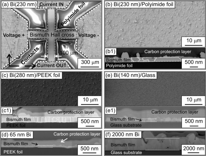
Figure 2.
a) Overview SEM image taken at the location of the Hall cross prepared at room temperature on the polyimide foil and subsequently post-annealed at 250 °C for 3 h. Electrical contacts are indicated in the image as well. The sensor element consists of a 230-nm-thick Bi layer. b) Magnified view of panel (a) revealing the morphology of the top surface of the Bi layer. c) SEM image of the top surface of the 280-nm-thick Bi film on flexible PEEK foil. e) Top view of the 140-nm-thick Bi on rigid glass. The panels (b1), (c1), and (e1) show the cross-section images of the respective samples prepared by FIB milling. Panels (d) and (f) reveal cross-section of the samples with 65- and 2000-nm-thick Bi, respectively.

