
Figure 5.
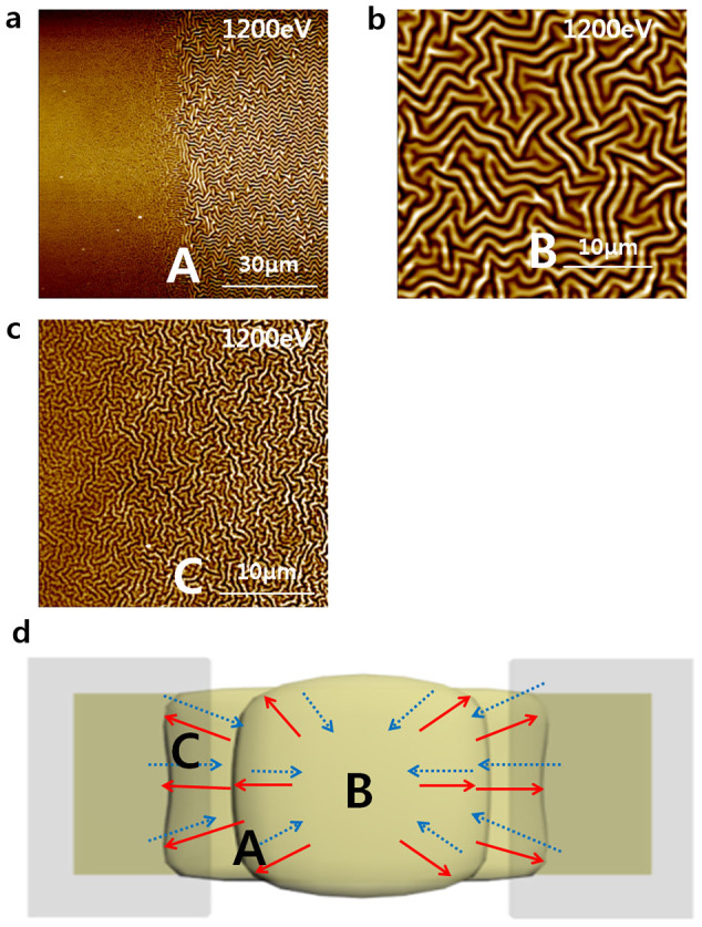
AFM images of wide-patterned PDMS films fabricated at IB powers of (a, b, and c) 1200 eV. The pattern width was 1 mm. (a) Interface between a region exposed to the IB irradiation (left-hand side) and a region not exposed to the IB irradiation. (b) Centre of a region exposed to the IB irradiation. (c) Region 80 μm from the edge of the exposure site. (d) Schematic illustration of the mechanism for the formation of wide-patterned PDMS films through IB treatment. The regions denoted by A, B, and C in (d) represent the regions shown in (a), (b) and (c), respectively.