Figure 6.
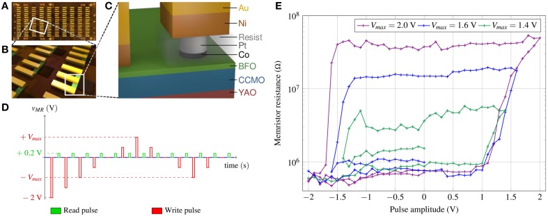
(A) Optical microscope image of the chip after patterning showing 5×10 ferroelectric tunnel junctions (FTJ); (B) 3D representation of a zoomed area containing a few FTJs. The three parallel bars are the ground-signal-ground contact pads; (C) 3D sketch of one FTJ (Boyn et al., 2014); (D) schema of the voltages applied to the memristor. The reading pulse Vread is lower than the threshold (Vread = 200 mV). Writing is performed by the application of 100 ns voltage pulses of different amplitudes. The writing voltages increase from −2 V to Vmax by a step of 0.1 V. Then, the amplitude of the writing pulses decreases to −Vmax; (E) dependence of the resistance of the ferroelectric tunnel memristor measured at Vread on the applied writing cycles. The different curves correspond to different consecutive measurements with varying Vmax.

