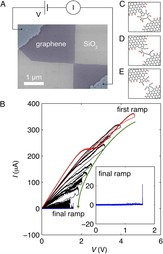
Fig. 1.
(A) Scanning electron micrograph of the graphene device. (B) Measured current–voltage characteristic of the full I–V trace. (Inset) I–V trace of the final voltage ramp before the formation of the nanogap. This exhibits a sharp increase of the conductance just before the nanogap forms. (C–E) Three atomic configurations with two (C), one (D), and zero (E) pathways.

