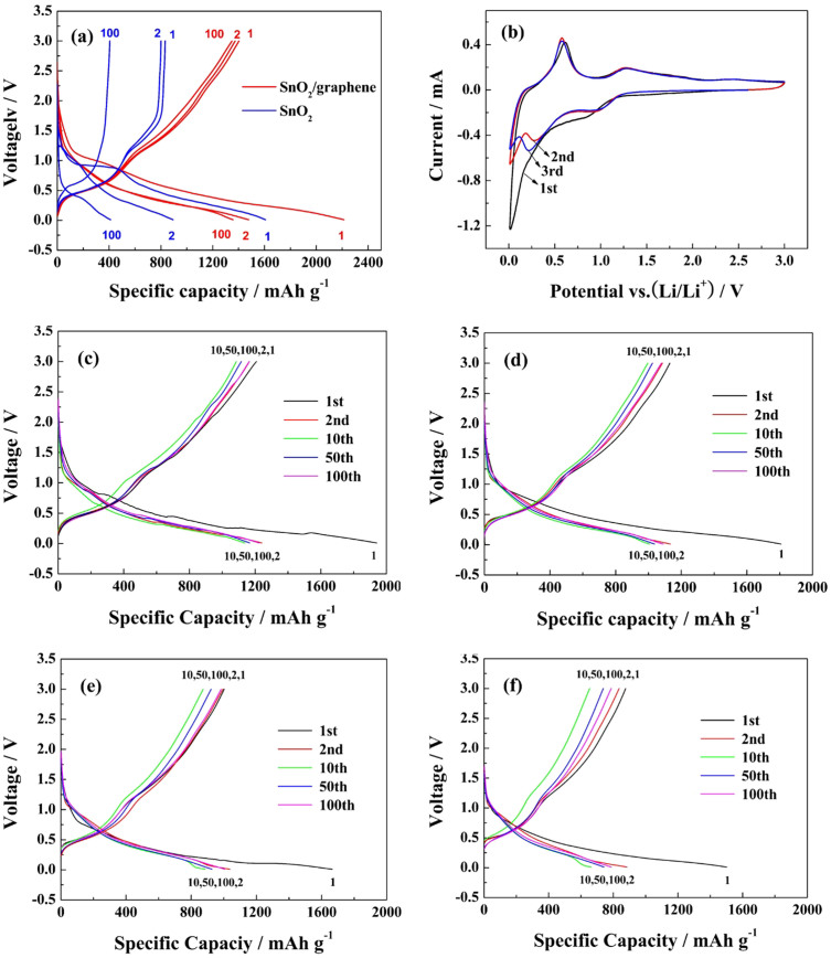
Figure 5. Discharge/charge profiles and CV curves.
(a) Discharge/charge profiles of SnO2 and SnO2/graphene at a current density of 100 mA g−1, and (b) CV curves of SnO2/graphene at a scanning rate of 0.1 mV s−1, (c) Discharge/charge profiles of SnO2/graphene at 300 mA g−1, (b) at 500 mA g−1, (c) at 700 mA g−1, and (d) at 1000 mA g−1.

