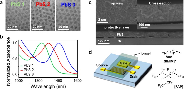
Figure 1.

(a) Transmission electron microscopy images of PbS 1 QDs (d ∼ 4.3 nm), PbS 2 QDs (d ∼ 4.6 nm), and PbS 3 QDs (d ∼ 5.1 nm) and (b) corresponding absorption spectra with λPbS1 = 1230 nm (green), λPbS2 = 1303 nm (red), and λPbS3 = 1407 nm (blue). (c) Scanning electron microscopy images of a five layer-by-layer PbS QD film. The top view image shows some surface cracks, the cross-section images reveal a homogeneous layer with a thickness of about ∼230 nm. (d) Schematic illustration of a PbS QD light-emitting field-effect transistor with a side-gate and an iongel electrolyte containing the ionic liquid [EMIM][FAP].
