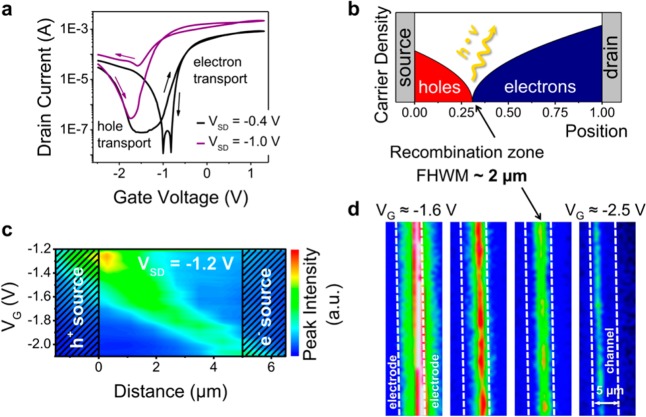
Figure 2.
(a) Typical transfer characteristics of an electrolyte-gated FET with spin-coated and ligand-exchanged PbS QDs indicating ambipolar transport. (b) Schematic illustration of hole and electron accumulation and recombination zone for a transistor in the ambipolar regime. (c) Position (distance from hole injecting electrode) and intensity of emission from a PbS QD FET (PbS 2 QDs, channel length L = 5 μm; integration time 10 s) depending on gate voltage for constant source-drain voltage (VSD = −1.2 V) and (d) false-color near-infrared images (wavelengths 800–1600 nm; integration time 5 s) of the recombination and emission zone from the same device at different gate voltages (VSD = −1 V); see also movie in Supporting Information D.

