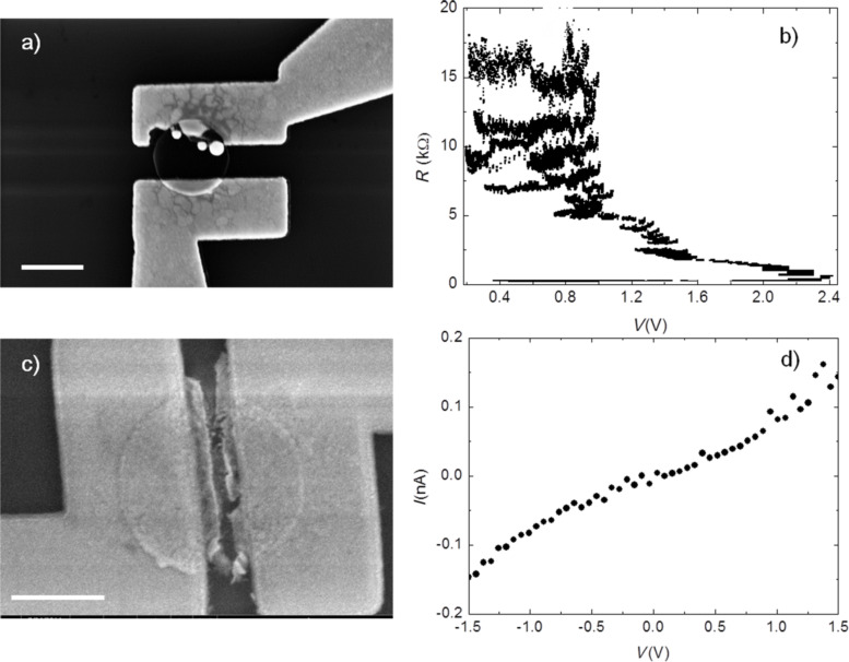
Figure 5.
a) SEM image of a non-patterned disc after the EB process. During EB the area around the graphene–metal contact gets heavily damaged due to high power dissipation at these spots. b) EB cycle for a patterned TG disc (see text) showing the transition from low-ohmic (≈200 Ω) to high-ohmic (≈20 kΩ) behavior, which indicates the opening of a gap. c) Corresponding SEM image showing intact metal contacts while a breaking is visible in the disc. d) I–V-characteristic of electroburned TG device. A tunneling current is visible, demonstrating the presence of an open gap in the range of a few nanometers only. The scale bar is always 1 µm.

