Figure 5.
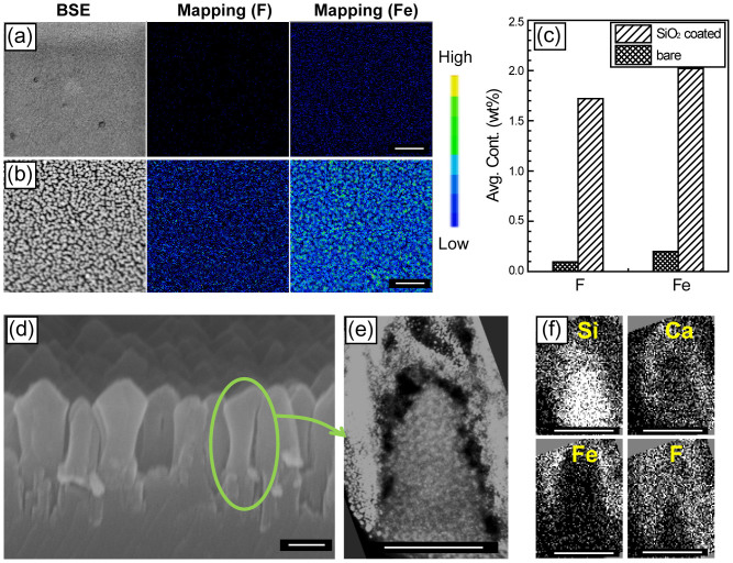
SEM image (left) and EPMA mapping (middle and right) analysis of glass surfaces for (a) SiO2-coated glass and (b) bare glass with F and Fe as the selected surface atoms. Scale bars are 1 μm. (c) EPMA intensity for Fe and F components on the samples in (a) and (b). (d) SEM image of nanostructured glass at an 80° tilt. Scale bar is 500 nm (e) TEM image of a single glass nanopillar and (f) its EELS area mapping of four components (Si, Ca, Fe, and F) where all components are false colored. (e) and (f) image scale bars are 300 nm

