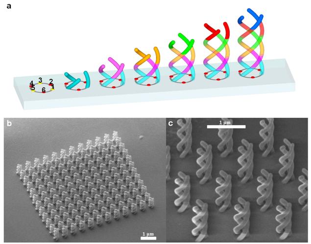
Figure 1. Device fabrication.
(a) Fabrication scheme to realize THNs. The basic two-dimensional layout consisting of an empty circle is divided in 6 sections (seeding sites arranged every 60°). During the first step, the circular motion of the beam leads to the 3D growth of three arches arranged every 120° (indicated with numbers 1,3,5). Then, after changing the starting angle from 0 ° to 60° anticlockwise the beam was moved to grow 3 arcs placed again every 120°. The extremely high level of alignment is achieved by setting the pattern parameters for a perfect overlap of consecutive arches. These two steps are repeated three times to get a complete loop of each sub-helix. (b) SEM images of the array showing THNs with ED=375 nm, WD=110 nm, VP=705 nm. The THN array size is 10 μm x10 μm, with LP=700 nm. (c) High magnification image of a small array area evidencing the wire continuity and high dimensional uniformity of THNs in all three spatial directions obtained by the TRG method.

