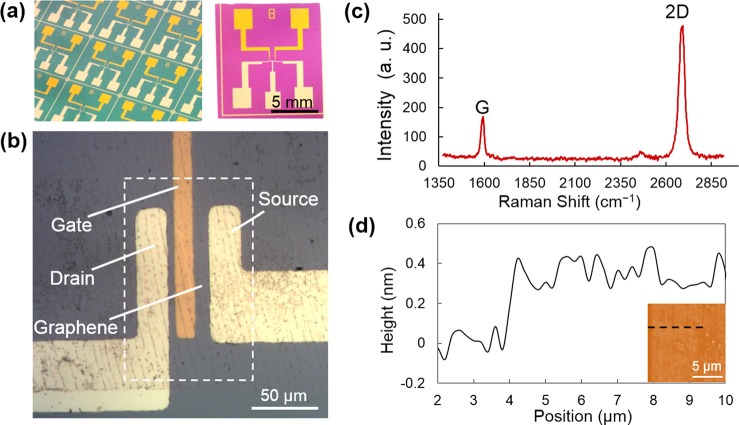
FIG. 2.
Micrographs of graphene nanosensors: (a) Multiple devices batch-fabricated on the same substrate (left) and close-up view of a single device (right). (b) Detailed view of the source, drain, and gate electrodes. Dashed box approximately indicates the region covered by graphene. (c) Raman spectrum of the graphene. (d) AFM measurements of the graphene thickness. Inset: AFM photo of graphene whose thickness was measured along the dashed line.

